Download
1 / 40
400 likes | 519 Views
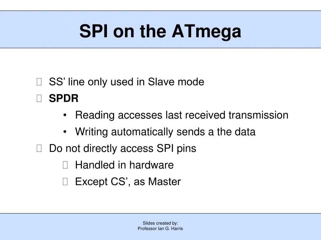
SPI on the ATmega. SS’ line only used in Slave mode SPDR Reading accesses last received transmission Writing automatically sends a the data Do not directly access SPI pins Handled in hardware Except CS’, as Master. Slides created by: Professor Ian G. Harris. SPI Pins on the ATmega.

E N D
SPI on the ATmega • SS’ line only used in Slave mode • SPDR • Reading accesses last received transmission • Writing automatically sends a the data • Do not directly access SPI pins • Handled in hardware • Except CS’, as Master Slides created by: Professor Ian G. Harris
SPI Pins on the ATmega • MISO, MOSI, and SCK are not explicitly accessed • HW handles pin access when SPDR is read/written • However, program must set directions on these pins • SS’ enables SPI in Slave mode Slides created by: Professor Ian G. Harris
SPI Registers • SPCR - SPI Control Register • Bit 7 - SPIE: SPI Interrupt Enable • Bit 6 - SPE: SPI Enable • Bit 5 - DORD: Data Order (1 = LSB) • Bit 4 - MSTR: Master/Slave Select (1 = master) • Bit 3 - CPOL: Clock Polarity • Bit 2 - CPHA: Clock Phase • Bits 1,0 – SPR1,SPR0: SPI Clock Rate Select Slides created by: Professor Ian G. Harris
SPI Registers • SPSR - SPI Status Register • Bit 7 - SPIF: SPI Interrupt Flag • Bit 6 - WCOL: Write Collision Flag • Bit 5:1 - Reserved • Bit 0: SPI2X: Double SPI Speed Bit Slides created by: Professor Ian G. Harris
SPI Clock Speed SPSR Bit 0 SPCR Bit 1 SPCR Bit 0 • Determines SCLK as a function of fosc Slides created by: Professor Ian G. Harris
SPI Master Example void SPI_MasterInit(void) { // Set MOSI and SCK output, all others input DDRB = (1<<DDB2)|(1<<DDB1); //Enable SPI, Master, set clock rate fosc/16 SPCR = (1<<SPE)|(1<<MSTR)|(1<<SPR0); } void SPI_MasterTransmit(char cData) { /* Start transmission */ SPDR = cData; /* Wait for transmission complete */ while(!(SPSR & (1<<SPIF))); } Slides created by: Professor Ian G. Harris
SPI Slave Example void SPI_SlaveInit(void) { //Set MISO output, all others input DDRB = (1<<DDB3); // Enable SPI SPCR = (1<<SPE); } char SPI_SlaveReceive(void) { // Wait for reception complete while(!(SPSR & (1<<SPIF))); // Return Data Register return SPDR; } Slides created by: Professor Ian G. Harris
I2C Protocol • Synchronous, serial protocol • Multiple masters, multiple slaves • Bitwidth is fixed, independent of number of slaves • Two wires: SDA (serial data) and SCL (serial clock) • Both lines are open-drain • Pulled up to high by default • State of bus is always known Slides created by: Professor Ian G. Harris
I2C Terminology • Master – Initiates and terminates transmission. Generates SCL. • Slave – Addressed by the Master • Transmitter – Placing data on the bus • Receiver – Reading data from the bus Slides created by: Professor Ian G. Harris
I2C Network Vcc Vcc SDA SCL Master Slave Master Slave Slave • SDA and SCL are bidirectional • Unlike SPI Slides created by: Professor Ian G. Harris
I2C Transaction Structure • Start Condition • Indicates the beginning of a transaction • Address/Direction Byte • Specifies slave for communication • Specifies read vs. write transaction • Data Byte(s) • Transmitted by either master or slave • Stop Condition • Indicates the end of a transaction Slides created by: Professor Ian G. Harris
Start and Stop Conditions SDA SDA SCL SCL Start Condition Stop Condition • Start Condition • Falling transition on SDA while SCL=1 • Stop Condition • Rising transition on SDA while SCL=1 Slides created by: Professor Ian G. Harris
Sending a Bit SDA SCL • SDA is sampled by receiver on the rising edge of SCL • SDA must be constant which SCL is high • Exception is Start/Stop Condition Slides created by: Professor Ian G. Harris
Acknowledge Bit SDA 2 8 3 1 ACK SCL • After each byte is sent, the receiver must acknowledge • Transmitter releases SDA, receiver must pull SDA low • Must be low for one pulse of SCL • If SDA is not pulled low, transmission is aborted Slides created by: Professor Ian G. Harris
Typical I2C Packet Address (7 bits) Data (8 bits) Start ACK Stop Direction Bit ACK • Each slave has an unique 7-bit address • Direction Bit: 0 indicates write, 1 indicated read • ACK bit after each byte Slides created by: Professor Ian G. Harris
I2C on ATmega • Two Wire Interface (TWI) is their name for it • Supports options which we will not consider • 10 bit addressing • Multi-master arbitration • Packet format is the same • Data sent MSB first Slides created by: Professor Ian G. Harris
TWI Module on ATmega Slides created by: Professor Ian G. Harris
Bit Rate Generator Unit • Generates the clock on SCL • Used only if acting as a Master • Controlled by two registers: • TWI Bit Rate Register (TWBR) • Prescalar bits in the TWI Status Register (TWSR) • fSCL = fosc / [16 + 2 (TWBR) * 4 TWPS] • fosc in slave >= 16 * fSCL Slides created by: Professor Ian G. Harris
Bus Interface Unit • TWI Address/Data Register (TWDR) • Contains the byte to send, of the byte received • START/STOP Controller • Not directly accessed by programmer • ACK/NACK Bit Register • Not directly accessed by programmer • Bus Arbitration Logic • Not directly accessed by programmer Slides created by: Professor Ian G. Harris
Address Match Unit • TWI Address Register (TWAR) • Contains the address of this device (in slave mode) • Incoming address (in TWDR) is compared to TWAR • TWI General Call Recognition Enable (TWGCRE) • Bit in TWAR which indicates that general call address (0000000) should be recognized • General call recognition allows broadcasts Slides created by: Professor Ian G. Harris
Control Unit • TWI Control Register (TWCR) • Used to set various I2C communication options • TWCR contains TWI Interrupt Flag (TWINT) • TWINT is set when an interesting TWI event occurs • Transmit START condition • Transmit address • Receive data byte • TWI Status Register (TWSR) • Contains status byte after TWINT is set Slides created by: Professor Ian G. Harris
Controlling TWI • Each transaction is divided into stages (“bus cycles”) • Cycles for a Write Transaction: 1. Send START, 2. Send Address, 3. Send Byte, 4. Send STOP • TWINT is automatically set and at the end of each stage • TWSR is also loaded with status of the cycle • Clearing TWINT is required to trigger the next bus cycle • TWINT is cleared by setting TWCR bit to 1 Slides created by: Professor Ian G. Harris
Write Transaction Example • Step 1: Send a START Condition void SendStart() { TWCR = (1<<TWINT)|(1<<TWSTA)|(1<<TWEN); } SendStart(); • TWEN bit enables TWI logic • TWSTA bit indicates START condition is next cycle • TWINT = 1 clears flag, initiating bus cycle Slides created by: Professor Ian G. Harris
Write Transaction Example • Step 1.5: Wait for START to be sent, check result void VerifyStatus(char code) { while (!(TWCR & (1<<TWINT))); if ((TWSR & 0xF8) != code) ERROR(); } VerifyStatus (START); • While statement waits for completion of START • TWSR, high 5 bits, should contain START (0x08) to indicate correct transmission Slides created by: Professor Ian G. Harris
Write Transaction Example • Step 2: Send Address void SendByte (char data) { TWDR = data; TWCR = (1<<TWINT) | (1<<TWEN); } SendByte(SLA_W); • SLA_Wis the slave address + direction bit • Since TWSTA is not set, TWDR will be transmitted Slides created by: Professor Ian G. Harris
Write Transaction Example • Step 2.5: Wait for Address to be sent, check result VerifyStatus(MT_SLA_ACK); • MT_SLA_ACK indicates that ACK was received Slides created by: Professor Ian G. Harris
Write Transaction Example • Step 3: Send Data, Wait for completion, Check result SendByte(DATA); VerifyStatus(MT_DATA_ACK); Slides created by: Professor Ian G. Harris
Write Transaction Example • Step 4: Send STOP Condition void SendStop() { TWCR = (1<<TWINT)|(1<<TWSTO)|(1<<TWEN); } SendStop(); Slides created by: Professor Ian G. Harris
TWI Interrupts • Example used while loops to wait for cycle completion • TWINT is set at the end of each cycle • Could have used interrupts to execute each stage • No need to waste processor time waiting Slides created by: Professor Ian G. Harris
I2C System Example Philips PCF8570 256 x 8-bit static low-voltage RAM with I2C-bus interface Interface with a RAM IC Slides created by: Professor Ian G. Harris
Memory IC Wiring • Address inputs are low bits of the address • High address bits are fixed • SDA, SCL attached to ATmega 2560 pins Slides created by: Professor Ian G. Harris
Memory Timing Diagrams • Timing diagrams are provided for transactions WRITE transaction, Master Transmitter, Slave Receiver • Need to write code to match the timing diagrams Slides created by: Professor Ian G. Harris
Write Transaction void WriteMTSR (char s_addr, char m_addr, char data) { SendStart(); VerifyStatus(START); SendByte(s_addr); VerifyStatus(MT_SLA_ACK); SendByte(m_addr); VerifyStatus(MT_DATA_ACK); SendByte(data); VerifyStatus(MT_DATA_ACK); SendStop(); } WriteMTSR(SLA_ADDR, MEM_ADDR, DATA); Slides created by: Professor Ian G. Harris
Analog to Digital Conversion (ADC) • Converts an analog voltage to a digital value • Maps input voltage range of digital values • Ex. 0V – 5V -> 0x00 – 0xFF • Allows the digital mC to use analog data • Can read analog sensors • Commonly built into mControllers • ATmega 2560 ADC has 10-bit accuracy • Digital value range 0 – 1023 Slides created by: Professor Ian G. Harris
Starting a Single Conversion • Set the AD Start Conversion (ADSC) bit in the AD Control and Status Register A (ADCSRA) • ADSC stays high as long as conversion is being performed • ADSC is cleared by HW when conversion is done • Use this to check for conversion completion Slides created by: Professor Ian G. Harris
Auto Triggering • May want to trigger conversion based on some event • Previous conversion completed • External interrupt • Timer interrupt • Set AD Auto Trigger Enable (ADATE) bit in ADCSRB register • Set AD Trigger Select (ADTS) bits to select trigger Slides created by: Professor Ian G. Harris
Auto Trigger Logic • AD Interrupt Flag (ADIF) enables “Free Running” mode Slides created by: Professor Ian G. Harris
ADC Clock Generation • Fast ADC clock – low conversion time, less accuracy • Slow ADC clock – high conversion time, more accuracy • AD Prescalar Select (ADPS) bits in ADCSRA • 50kHz – 200kHz is needed (up to 1000kHz) Slides created by: Professor Ian G. Harris
Channel/Reference Selection • Analog source can be any pin from PortF or PortK • Source channel selected by MUXn bits in ADMUX register • Reference voltage can be Vcc, 2.56V, 1.1V • Reference selected by REFS bits in ADMUX • Changes during a conversion take effect after the conversion Slides created by: Professor Ian G. Harris
ADC Conversion Result • Result is contained in ADCL and ADCH registers • 10-bits contained in 2 registers, 6 bits ignored • ADLAR bit in ADMUX determines left (right) adjust • Left adjust – ignore low 6 bits of ADCL • Right adjust – ignore high 6 bits of ADCH • If 8-bit accuracy is enough, choose left adjust and ignore ADCL Slides created by: Professor Ian G. Harris