Download
1 / 74
770 likes | 1.02k Views
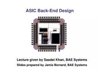
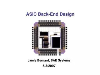
ASIC Back-End Design. Jamie Bernard, BAE Systems 5/3/2007. Agenda. Introduction Design Flow Overview Floorplan Timing Driven Placement Clock Tree Synthesis Routing Verification Design Example. Introduction. Introduction. Technological Advances 19 th Century - Steel

E N D
ASIC Back-End Design Jamie Bernard, BAE Systems 5/3/2007
Agenda • Introduction • Design Flow • Overview • Floorplan • Timing Driven Placement • Clock Tree Synthesis • Routing • Verification • Design Example
Introduction • Technological Advances • 19th Century - Steel • 20th Century – Silicon • Growth in Microelectronic (Silicon) Technology • Moore’s Law (# of transistors double/18 months) • One Transistor • Small Scale Integration (SSI) • Multiple Devices (Transistor / Resistor / Diodes) • Possibility to create more than one logic gate (Inverter, etc) • Large Scale Integration (LSI) • Systems with at least 1000 logic gates (Several thousand transistors) • Very Large Scale Integration • Millions to hundreds of millions of transistors (Microprocessors) • Intel indicates that dual core processors will soon exist that contain 1 billion transistors
Introduction • Manual (Human) design can occur with small number of transistors • As number of transistors increase through SSI and VLSI, the amount of evaluation and decision making would become overwhelming (Trade-offs) • Maintaining performance requirements (Power / Speed / Area) • Design and implementation times become impractical • How does one create a complex electronic design consisting of millions of transistors? Automate the Process using Computer-Aided Design (CAD) Tools
Introduction • CAD tools provide several advantages • Ability to evaluate complex conditions in which solving one problem creates other problems • Use analytical methods to assess the cost of a decision • Use synthesis methods to help provide a solution • Allows the process of proposing and analyzing solutions to occur at the same time • Electronic Design Automation • Using CAD tools to create complex electronic designs (ECAD) • Several companies who specialize in EDA • Cadence® Design Systems • Magma® Design Automation Inc. • Synopsys® CAD Tools Allow Large Problems to be Solved
Design Flow - Overview • Generic VLSI Design Flow from System Specification to Fabrication and Testing • Steps prior to Circuit/Physical design are part of the FRONT-END flow • Physical Level Design is part of the BACK-END flow • Physical Design is also known as “Place and Route” • CAD tools are involved in all stages of VLSI design flow • Different tools can be used at different stages due to EDA common data formats* • Synopsys® CAD tool for Physical Design is called Astro™
Where does the Gate Level Netlist come from?1st Input to Astro™
Standard Cell Library2nd Input to Astro™ • Pre-designed collection of logic functions • OR, AND, XOR, etc • Contains both Layout and Abstract views • Layout (CEL) contains drawn mask layers required for fabrication • Abstract (FRAM) contains only minimal data needed for Astro™ • Timing information • Cell Delay / Pin Capacitance • Common height for placement purposes
Basic Devices and Interconnect • Integrated circuits are built out of active and passive components, also called devices: • Active devices • Transistors • Diodes • Passive devices • Resistors • Capacitors • Devices are connected together with polysiliconormetal interconnect: • Interconnect can add unwanted or parasitic capacitance, resistance and inductance effects • Device types and sizes are process or technology specific: • The focus here is on CMOS technology 38
VDD PMOS OUT IN OUT IN NMOS GND Gate Schematic Transistor or Device View Transistor or Device Representation CMOS Inverter Example Gates are made up of active devices or transistors. 37
VDD VDD PMOS PMOS OUT IN IN OUT NMOS NMOS GND GND Transistor or Device View Physical or Layout View What is “Physical Layout”? CMOS Inverter Example Physical Layout – Topography of devices and interconnects, made up of polygons that represent different layers of material. 39
Silicon Substrate Layout or Mask (aerial) view Process of Device Fabrication • Devices are fabricated vertically on a silicon substrate wafer by layering different materials in specific locations and shapes on top of each other • Each of many process masks defines the shapes and locations of a specific layer of material (diffusion, polysilicon, metal, contact, etc) • Mask shapes, derived from the layout view, are transformed to silicon via photolithographic and chemical processes Wafer (cross-sectional) view 40
0.25 um Input PMOS VDD Output GND NMOS Aerial or Layout View Wafer Representation of Layout Polygons Wafer Cross-sectional View Example of complimentary devices in 0.25 um CMOS technology or process. 41
Metal 1 Metal 1 Oxide insulation Poly Diffusion Diffusion VDD IN GND Contacts: Connecting Metal 1 to Poly/Diff’n Diffusion, Poly and Metal layers are separated by insulating oxide. Connecting from Poly or Diffusion to Metal 1 requires a contact or cut. Cut or Contact (a hole in the oxide) 49
Length L Length L Narrower Width = Lower current through channel Wider Width = Higher current through channel G A T E G A T E W Width (W) Width What is meant by “0.xx um Technology”? Gate or Channel Dimensions (L and W) - In CMOS Technology the um or nm dimension refers to the channel length, a minimum dimension which is fixed for most devices in the same library. - Current flow or drive strength of the device is proportional to W/L; Device size or area is proportional to W x L. 42
Comparing Technologies L = 0.5 um L = 0.25 um 2L 2L W = 3 um 2L 2L W = 1.5 um A: 0.5 um Technology Area Comparison B: 0.25 um Technology The drive strength of both devices is the same: W/L = 6. The diffusion area (5xLxW) of A is 4x that of B. Which is preferred? 43
0.25 um IN 0.25 um L = 0.25 um IN IN 3 um OUT OUT OUT W = 1.5 um 1.5 um GND GND GND “2X” NMOS (W/L = 12) “2X” NMOS (W/L = 6 + 6) Relative Device Drive Strengths “1X” NMOS (W/L = 6) To double the drive strength of a device, double the channel width (W), or connect two 1X devices in parallel. The latter approach keeps the height at a fixed or “standard” height. 44
Input Input Output Output Gate Drive Strength Example inv2 inv1 2x 1x PMOS transistor Parallel PMOS transistors NMOS transistor Parallel NMOS transistors Each gate in the library is represented by multiple cells with different drive strengths for effective speed vs. area optimization. 45
2x 1x 1x 1x 1x Drive/Buffering Rules: Max Transition/Cap Upsized DriverorAdded Buffers After Optimization Before Optimization Maximum Transition Rule Violation Maximum Transition Rule Met 46
Timing Constraints3rd Input to Astro™ • Derived from system specifications and implementation of design • Identical to timing constraints used during logic synthesis • Common constraints in electronic designs • Clock Speed/Frequency • Input / Output Delays associated with I/O signals • Multicycle Paths • False Paths • Astro™ uses these constraints to consider timing during each stage of the place and route process
Concept of Place and Route • Location of all standard cells is automatically chosen by the tool during placement (Based upon routing and timing) • Pins are physically connected during routing (Based upon timing)
Concepts of Placement • Standard cells are placed in “placement rows” • Cells in a timing-critical path are placed close together to reduce routing related delays (Timing Driven) • Placement rows can be abutting or non-abutting
Concepts of Routing • Connecting between metal layers requires one or more “vias” • Metal Layers have preferred routing directions • Metal 1 (Blue) Horizontal • Metal 2 (Yellow) Vertical • Metal 3 (Red) Horizontal
Design Flow – Floorplan • Layout design done at the chip level • Defining layout hierarchy • Estimation of required design area • A blueprint showing the placement of major components in the design (non-standard cell) • Inputs / Output (I/O) • RAMs / ROMs/ • Reusable Intellectual Property (IP) macros • Approaches to Floorplanning (Automatic or Manual) • Constructive • Iterative • Knowledge-Based
Design Must Be Floorplanned Before P&R • Floorplan of design: • Core area defined with large macros placed • Periphery area defined with I/O macros placed • Power and Ground Grid (Rings and Straps) established • Utilization: • The percentage of the core that is used by placed standard cells and macros • Goal of 100%, typically 80-85%
I/O Placement and Chip Package Requirements • Some Bond Wire requirements: • No Crossing • Minimum Spacing • Maximum Angle • Maximum Length
Guidelines for a Good Floorplan • A few quick iterations of place and route with timing checks may reveal the need for a different floorplan
Defining the Power/Ground Grid and Blockages • Purpose of Grid is to take the VDD and VSS received from the I/O area and distribute it over the core area • Blockages can also be added in the floorplan to prohibit standards cells from being placed in those areas
Design Flow – Timing Driven Placement • Astro™ optimizes, places, and routes the logic gates to meet all timing constraints • Balancing design requirements • Timing • Area • Power • Signal Integrity
Timing Constraints • Astro™ needs constraints to understand the timing intentions • Arrival time of inputs • Required arrival time at outputs • Clock period • Constraints come from the Logic Synthesis tool • SDC (Synopsys Design Constraints) format
Cell and Net Delays • Astro™ calculates delay for every cell and every net • To calculate delays, Astro™ needs to know the resistance and capacitance of each net • Uses geometry of net and Look Up Tables to estimate the resistances and capacitances
Timing Driven Placement • Timing Driven Placement places critical path cells close together to reduce net RC • Prior to routing, RC are based on Virtual Routes • What if critical paths do not meet timing constraints with placement?
Logic Optimizations • These optimizations can be done during pre-place, in-place, or post-place stages of placement • Each optimization can be done separately or all done concurrently during placement (none – one – all)
Design Flow – Clock Tree Synthesis • All clock pins are driven by a single clock source • Large delay and transition time due to length of net • Clock signal reach some registers before others (Skew)
Clock Tree Topologies • Clock source is connected to center of the network • Networks are distributed in a H or X shape until clock pin of register is driven by a local buffer H-Tree and X-Tree Topologies Solve Single Clock Pin Problem
After Clock Tree Synthesis • A clock (buffer) tree is built to balance the output loads and minimize the clock skew • A delay line can be added to the network to meet the minimum insertion delay (clock balancing)
Gated - CTS • Clocks may not be generated directly from I/O • Power saving techniques such as clock-gating are used to turn of the clock to sections of the design • Astro™ can interpret gated clocks and can build clock trees “through” the logic to the registers
Effects of CTS • Several (Hundreds/Thousands) of clock buffers added to the design • Placement / Routing congestion may increase • Non-clock cells may have been moved to less ideal locations • Timing violations can be introduced
Design Flow – Routing • Routing is a fundamental step in the place and route process • Create metal shapes that meet the requirements of a fabrication process • The physical connection between cells in the design • Virtual routes used during placement and CTS need to become reality • Timing of design needs to be preserved • Timing data such as signal transitions and clock skew needs to match the virtual route estimates Process of Routing Can Be Timing Driven
Timing Driven Routing • Routing along the timing-critical path is given priority • Creates shorter, faster connections • Non-critical paths are routed around critical areas • Reduces routing congestion problems for critical paths • Does not adversely impact timing of non-critical paths
Concept of Routing Tracks • Metal routes must meet minimum width and spacing “design rules” to prevent open and short circuits during fabrication • In grid based routing systems, these design rules determine the minimum center-to-center distance for each metal layer (Track/Grid spacing) • Congestion occurs if there are more wires to be routed than available tracks
Grid-Based Routing System • Metal traces (routes) are built along and centered around routing tracks • Each metal layer has its own tracks and preferred routing direction • Metal 1 – Horizontal • Metal 2 – Vertical • Track and pitch information can be located in the technology file • Design Rules