Download
1 / 30
300 likes | 429 Views
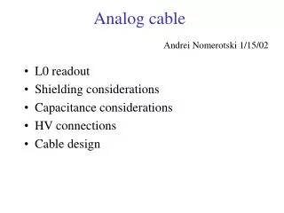
Goals SVX4 chip Overview of Run 2B readout Analog flex cable Hybrids Interfacing to Run 2A readout Performance issues Summary. D0 Run 2B Silicon Electronics Andrei Nomerotski, Fermilab December 3 rd 2001, Technical Design Review. Robust system based on new SVX4 chip Run 2A readout

E N D
Goals SVX4 chip Overview of Run 2B readout Analog flex cable Hybrids Interfacing to Run 2A readout Performance issues Summary D0 Run 2B Silicon ElectronicsAndrei Nomerotski, FermilabDecember 3rd 2001, Technical Design Review
Robust system based on new SVX4 chip Run 2A readout Minimize time, effort and cost Minimum R&D Recycle Run 2A readout as much as possible Conservative, low risk solutions Simple production, testing and commissioning Use Run2A commissioning experience Goals
SVX4 Chip • New chip : SVX4 • Designed by Fermilab/LBL/Padua • 0.25 mm technology, intrinsically radiation hard • Based on SVX3, compatible with SVX2 • Several new schematics solutions • D0 will use differential readout • Use the same pad ring as CDF • D0 DAQ can operate with SVX3 chips • D0 DAQ was designed for SVX2 • Some remapping of control signals is required • Tested in Nov 2000, one SVX3 chip was read out with D0 Sequencer SVX3 Address & Data, 128 channels
SVX4 Chip • Front End : • positive polarity • gain 3 mV/fC, 5% uniformity • load 10 – 40 pF • risetime 60-100 nsec • dynamic range 200 fC • ‘black hole’ clumping • reset time 200 nsec • pipeline 42 cells • Back End : • Wilkinson ADC, 106 MHz counter • dynamic pedestal subtraction • data sparsification • neighbor logic • differential output drivers upto 17 mA • configuration register
SVX4 Chip • Test chip submitted to MOSIS in June 2001, back in August • 16 channels LBL design preamp + pipeline • 48 channels FNAL design preamp + pipeline • Common bias preamp + pipeline as in SVX3 • 12 different input transistor sizes used to optimize noise • Results: • Optimum preamp ENC = 450e + 43.0e/pF • Pipeline works • Excellent radiation hardness • Full chip layout and simulation in progress • Submission of prototypes Dec 21st 2001 • Two versions for prototyping • Conservative • On-chip bypassing of analog voltage • Chips available for tests in March 2002 • Joint test effort of CDF & D0 at LBL and Fermilab • Important to test prototypes as extensively as possible • Second prototype submission will get the chip on the critical path! • Production run planned in July 2002 LBL Pre-amp Pipeline FNAL Pre-amp
Silicon Detector Layout Positioning bulkhead Cooling bulkheads Junction cards
Layers 1 - 5 Readout • On-board double-ended beryllia hybrid • Reduction of cables is achieved by • Analog ganging : connected strips in L2-5 • Digital ganging : chips bonded to different sensors are daisy chained on hybrid in L1-5 • Low mass digital flex cable with connectors on both sides
Layer 0 Readout • small radius & minimal material => flex analog cables • flex length is equalized • two-chip hybrids, no ganging • beyond hybrid : identical to L1 • challenging : • noise performance • manufacturing and assembly
Cable Count Cannot exceed Run 2A cable count Layer SVX4/Hybrid # cables 0 2 144 1 6 72 2 10 96 3 10 144 4 10 192 5 10 240 all layers 888 Run 2A 912 # of sensors and cables per layer
Signal level translation 5 V – 2.5 V Tight spec on 2.5 V (2.25 – 2.75 V) => Voltage regulation Mapping between SVX4 and SVX2 Differential / Single-Ended translation Changes of Run 2A Readout Modifications :
Preserve Run 2A segmentation of readout : One hybrid is an independent unit (separate cable) up to an accessible region. Proven to be successful during Run 2A commissioning. Jumper Cable - Junction Card - Twisted Pair Cable – Adapter Card New Adapter Card is active, implements necessary modifications Junction Cards are located in an accessible area Twisted Pair Cable is well suited for differential SVX4 readout Round cable facilitates routing on the face of the calorimeter Run 2B Readout
Analog Flex Cables • Low mass, fine pitch cables for Layer 0 • Dyconex (Switzerland) • Good previous experience • D0 has collaborators in Zurich • In Oct 2001 delivered 25 pre-prototype cables, • Used new technology : thermal imaging with IR sensitive photoresist, feature size 3-4 um • Cables are CDF L00 proxies • 128 traces, trace width 6-7 mm • Mixed 50 and 100 um pitch with fanout regions, total trace length ~42 cm • 2 rows of gold plated bond pads
Analog Flex Cables • Test results • Good quality of imaging • Good quality of 2 cables without gold on bond pads • 3 opens, no shorts • Uniform characteristics across cable, R ~ 5 Ohm/cm • Poor quality of gold plated cables • Many opens in fanout region • Many shorts between bond pads after gold plating • Possible solution • Less aggressive design • Wider traces 15-20 um • Constant 100 um pitch without fanout region • Two cables shifted by 50 um, effective pitch 50 um • Glued to substrates to allow for bonding • Investigating other vendors • What about performance ?
Analog Flex Cables • Capacitive load • Typically C = 0.25 – 0.5 pF/cm • Compares to 1.0 - 1.2 pF/cm in silicon • Simple analytical calculations agree with measurements within 20% • 100 um pitch, 16 um trace width cable has C comparable to L00 cable • Doing finite element calculations to confirm Capacitance versus Trace Width
Noise calculation Max length of analog cable ~ 45 cm Takes into account Capacitive load Serial resistance Leakage current after 15 fb-1 Good noise performance Better performance of SVX4 wrt SVX3 Analog Flex Cable S/N versus Temperature 4 different cable lengths
Hybrids • Based on Beryllia ceramic, ~0.4 mm thick • Minimize material • Good heat conductor • Established technique, possible vendor CPT, Oceanside CA • Multilayer structure on the substrate • six Au layers • GND & power planes, 4 um thick • Traces, 8 um thick, 100 um wide • five 40 um dielectric layers • Two technologies for vias in dielectric • Etching (Fodel dielectric), min via size 4 mils • Screen printing, min via size 8 mils • Screen printing is our baseline • Cost effective • More vendors available
Hybrids • Four types of hybrids • Layer 0 : 2 chips • Layer 1 : 6 chips, double-ended • Layers 2-5 : 10 chips, double-ended • Axial • Stereo, different width, electrically identical to axial • For each hybrid (Layers 1-5) • ~10 mil spacing between vias => screen printing • 50 pin AVX 5046 connector, 3 mm high • Allows for easy testing during all phases of production and assembly • Used by CDF for Run 2A SVX • bypass capacitors, termination resistors • temperature sensor • HV routed to side pin with 4 neighbors removed, tested to 1600 V • Reserved space (“nuts”) for assembling purposes • Ready to order prototypes for Layer 1 Layer 1 hybrid layout
Hybrids • Layers 2-5 10-chip hybrid • Design similar to Layer 1 6-chip hybrid • Same connector pinout • Same jumper cable design Layer 2-5 stereo hybrid Top metal layer
Digital Jumper Cable Hybrid - Jumper Cable - Junction Card - Twisted Pair Cable – Adapter Card Cross section of Jumper Cable • Same design for L1–5 • 6-8 different lengths, max length ~ 1 m • Kapton substrate, width 14.7 mm, thickness 130 um • Line width 125 um, thickness 33 um • HV on the same cable • AVX 50-pin connector on both sides
Junction Card Hybrid -Jumper Cable - Junction Card - Twisted Pair Cable – Adapter Card • Conceptual design ready • L0-1 : 3 hybrids junction card L2-5 : 4 hybrids junction card • 50-pin AVX connectors, three plug heights: 3.5, 4.0, 4.5 mm • Twisted pairs are soldered to JC, cards are extensions of cable bundles • Dimensions 70 mm x 25 mm Top view of L0-1 Junction Card
Twisted Pair Cable Hybrid -Jumper Cable - Junction Card - Twisted Pair Cable – Adapter Card • Conceptual design ready • Dense assembly (OD 5-7 mm) with • Twisted pairs : total 21; 44-pin 0.625 mm dual row Omnetics connector • differential signals • single-ended signals • Temperature, voltage sensing, spares • Common shield • Connectors can be purchased terminated with twisted pairs • Power and HV lines • Clock mini-coaxial cables • Round cross section – easy to route between Junction Cards and Adapter Cards Hybrid 1 signals Hybrid 1 power & HV Junction Card Hybrid 2 signals Hybrid 2 power & HV Hybrid 3 signals Hybrid 3 power & HV L0-1 Junction Card – Twisted Pair Cable Assembly
Conceptual design ready Adapter Card is active : Two voltage regulators per hybrid: analog and digital voltages Differential-to-Single-Ended 2.5-to-5 V translation for SVX4 Data 5-to-2.5 V translation for SVX4 Controls Routing of Clock and HV Three rings of Adapter Cards at two ends of calorimeter Option A : 37 x 3 4-channel ACs Option B : 34 x 3 4- and 6-channel ACs Adapter Card Hybrid -Jumper Cable - Junction Card - Twisted Pair Cable – Adapter Card Top view of 4-channel Adapter Card
Baseline : retain Run 2A IB’s, use in full functionality Signal regeneration and termination LV distribution LV voltage/current monitoring HV distribution for L2-5 (< 300 V) Hybrid Enable/Disable Hybrid temperature monitoring Present IB fixes several SVX2 “features” Assumption : SVX4 will not have new “features” which cannot be recovered with present IB Otherwise will need new IB Move LV power supplies to Platform Allows for maintenance during short Controlled Accesses to Collision Hall Replace bulk supplies with smaller ~ 7 A supplies Voltage regulators at Adapter Card make increased length of the path acceptable Interface Board & Power Supplies
To keep up with radiation damage Increased depletion voltage Current few mA / sensor strong function of temperature 1000 V spec for L0-1 300 V spec for L2-5 One HV channel per hybrid will have up to 4 sensors per HV channel in L4-5, 2 sensors in L1 Splitting of channels possible in outer layers Two options : Keep present BiRa system Meets the specifications Must split for outer layers Buy a new system (ex. CAEN) Need redesign HV distribution path from Counting House to Collision Hall High Voltage
Readout time is important issue in deadtime accounting Simulations : Two-jet events Run 2B GEANT Realistic clustering Neighbors and noise contribution Maximum # of strips read out per cable Allows for comparison between layers Readout time is comparable for first three layers Assumes low S/N in Layer 0 after radiation damage Justifies 2-chip readout for Layer 0 Deadtime is still dominated by digitization and pipeline reset ( ~7.2 usec). Total, ~11-12 usec, is acceptable. Performance issues
New readout is based on SVX4 and Run2A system Status of main components SVX4 : good progress But : schedule depends on single submission Analog flex cables : looking for simple solutions Hybrids & Digital flex cables : good progress, ready to prototype Interfacing to Run 2A electronics : have a baseline design Power Supplies & HV: need to define a baseline Short term focus on items close to the critical path SVX4 testing Hybrids Moved beyond conceptual design : ready to prototype Summary
Dynamic range >200 fC = 50 MIPs Preamp is reset once a beam revolution => after ~ 450 ppbar interactions at high L Preamp saturation will cause inefficiency Checked with full GEANT simulation 1% of channels receive > 25 MIPs (100 fC) 200 fC dynamic range is adequate SVX4 Chip
Shielding of the cable Common mode noise potentially a problem Guard ring structure or ground plane ? Total thickness of 12 cables < 3-4 mm C calculations for 50 um pitch cable with a ground plane Capacitance under control if ground plane is >100 um away Analog Flex Cable Capacitance versus distance to GND plane GND plane
SVX4 has side bond pads AVDD & DVDD, DGND AVDD bypass capacitor VCAL One more capacitor necessary for preamp Two resistors to set ADC parameters Priority_IN and _OUT, Top/Bottom Neighbor Finger between chips allows for bonding 0.5 mm alumina ceramic One (or two) metal layer design 4 surface mounted components Can be simpler if on-chip bypassing works SVX4 Finger
Hybrids • AVX connector pinout • Same for Layers 1 – 5