Download
1 / 41
460 likes | 749 Views
The Future Of Memory And Storage: Closing The Gap. Dean A. Klein VP Market Development Micron Technology, Inc. Key Takeaways. Understand the CPU-to-memory gap Understand issues and opportunities to fill the CPU-to-memory gap Understand the memory to storage gap

E N D
The Future Of Memory And Storage: Closing The Gap Dean A. Klein VP Market Development Micron Technology, Inc.
Key Takeaways • Understand the CPU-to-memory gap • Understand issues and opportunities to fill the CPU-to-memory gap • Understand the memory to storage gap • Understand issues and opportunities to fill the memory-to-storage gap
Processor Trends • Increasing core performance • Increasing cores • Increasing bus speed • More memory
Memory Trends • Increasing density • Faster interfaces • Increasing latency • NAND Memory Transfer Rate chart: Micron research
Growing Gaps 1B 100M 10M 1M Clocks of Latency 1000 100 10 1 Source: Instat, Micron, Intel
Level 1 Cache Level 3 Cache Level 2 Cache Main Memory Disk NAND Flash Memory Hierarchy Expansion
Processor Trends • AMD “Barcelona” • Quad core • 2M shared L3 cache • Dedicated L2 caches • Intel “Penryn” • Dual/Quad core • 6MB/12MB L2 cache • Intel “Nehalem” • Quad/8 core
Main Memory Data Rate Trends • DRAM bandwidth typically doubles every 3 years NGM Diff NGM SE DDR2 DDR SDRAM DDR3
Memory Trends • But Latency is actually getting WORSE… • And power is a problem… • What drives memory evolution today? Economics and Physics
Economics Drives Memory DRAM Market Price-per-bit Decline (Normalized- Millicent/bit) 1979 1980 Price per Bit (Millicents) 1981 1984 1982 1988 1983 1989 1985 1990 1987 1993 1986 1995 1991 1994 1992 1996 1997 2000 1998 1999 Historical price-per-bit decline has averaged 35.5% (1978 - 2002) 2003 2004F 2001 2006F 2002 2005F 2008F 2007F 100,000,000 1,000,000 10,000 100 1 Cumulative Bit Volume (1012)
DRAM Cell Layout: 8F2 2F 4F Source: CMOS Circuit Design , Layout, and Simulation - Baker
SRAM Cell Layout: 140F2 Source: CMOS Circuit Design , Layout, and Simulation - Baker
Compared Source: CMOS Circuit Design , Layout, and Simulation - Baker
Cell Sizes Compared Source: Micron Market Research
Power Trends Idle Active Active Idle • X16 devices at nominal Vdd, linear trendlines
Voltage Scaling Trends 7 6 5 4 3 2 1 0 1990 1995 2000 2005 2010
Process Cost Increasing Cost per Gigabit Years by quarter
Options For L3 Cache • SRAM L3
DRAM Can Be Fast Random 16Byte Transfers Max Envelope 4,000 3,500 3,000 2,500 2,000 Bandwidth per device (MBps / dev) 1,500 1,000 DDR2 500 DDR3 GDDR3 0 RLDRAM Access pattern: 8 READS followed by 8 WRITES
Through-Wafer Interconnect • Reduced parasitic loads • Smaller ESD structures • Greater numbers of interconnects • TWI
Redistribution Layers • Allow layout flexibility • Reduced parasitic loads • Supports great numbers of interconnects • RDL
Stacked Silicon • Goal of TWI and RDL • Supports N≥2 layers of silicon • Supports processes optimized for device
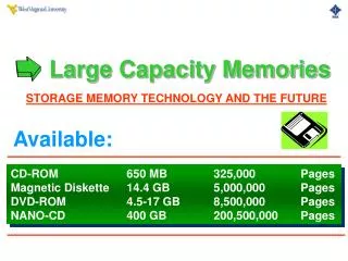
Storage Demand • 161exabytes of digital data were generatedin 2006 • That’s about 168 million terabytes, or roughly equivalent of 36billion digital movies 1 million copiesof every book in the Library of Congress 43trilliondigitalsongs Sources: IDC, UC Berkeley, CIA World Fact Book, USA TODAY Research
DRAM To Disk Evolution • “Flash is Disk, Disk is Tape”? • Performance, not capacity, is the issue • Disk will continue as the $/bit leader • NAND pricing is on a steep decline
NAND Density Trends • Beating Moore’s Law HDD, NAND Flash Pricing (Log Chart) $100 $43.39 $15.66 $7.12 $10 $4.68 $3.76 $3.11 $2.05 $1.96 $1.34 $1.08 $1.02 $0.89 $1 $1.30 $1.02 $0.81 $0.58 $0.45 HDD 0.85in, 1.0in, 1.8in Combined NAND Flash Mobile HDD 2.5in (portable PCs) $0.35 $0 2007 2008 2009 2010 $/GB 2005 2006 Source: IDC 2007
SSDs In The Enterprise CPU RelativeLatency RelativeCost/bit NAND NAND Flash Closes the Latency Gap Cost/bit Data as of Aug ‘06
Datacenter Issues • Power • Reliability • Space • Performance Source: Microsoft Research
Management Stack Application • Flash Translation Layer • Interfaces to traditional HDD File System • Enables sector I/O to Flash • Wear leveling • Bad block management • Automatic reclamation of erased blocks • Power loss protection • Manages multiple NAND devices Operating System File System HDD SSD Flash Translation Layer (FTL) Controller • Controller • Manages Physical Protocol • NAND Command encoding • High Speed data transport (DMA/FIFO) ECC Controller ECC • Error Control • Algorithm to control sector-level bit reliability • Implemented in hardware with software control • Algorithm depends upon Flash technology NAND
SSD Quality And Reliability • NAND • Extended operation of NAND • On-going production management to assure reliability • Management • NAND-Validated Error Correction • Static and dynamic Wear Leveling • Garbage collection • Bad block remapping • Other proprietary schemes Applications • Optimizations based upon Management and NAND • SSD Specs • 10 Year operating life • 10-15 Bit Error Rate • 1E+6 hours MTBF • NAND Specs • 100K P/E Cycles • 1-Bit ECC • Limited Read Cycles • 10 year data retention
App's Target BER Zone ECC Code Selection Becoming More Important • As the raw NAND Flash BER increases, matching the ECC to the application’s target BER becomes more important 1.0E-25 t = 5 t = 3 t = 4 t = 6 t = 2 t = 1 1.0E-23 1.0E-21 1.0E-19 For SLC A code with correction threshold of 1 is sufficient 1.0E-17 1.0E-15 Application Bit Error Rate t = 0 1.0E-13 1.0E-11 t = 4 required (as a minimum) for MLC 1.0E-09 1.0E-07 1.0E-05 1.0E-03 1.0E-01 1.0E-01 1.0E-03 1.0E-05 1.0E-07 1.0E-09 1.0E-11 1.0E-13 1.0E-15 Raw NAND Bit Error Rate
Endurance: Usage Example Continuous write at max bus speed of 100MB/s with a 5:1 r/w ratio 30 minutes to fill up disk 50 years before 1M I/O cycle limit is exceeded 250 years before 1M I/O cycle limit is exceeded Capacity: 32 GB At 20% utilization Opportunities for improvement, i.e. new coding, will further extend time to cycle limit Flash Drives are ready for deployment for various applications
Meaningful Cycling Metrics • Practical, testable solutions are needed • Simply stating that “the drive must meet 1 million complete read and write cycles” is not realistic 1M 100K Years for one completepass Cycles 10K 13 1K Capacity (%) 100%
Cycling For CE Applications 1M Years for one completepass 0.93 100K Cycles 10K 1K 5% 20% 75% Capacity (%)
Cycling For Servers 1M Years for one completepass 3.02 100K Cycles 10K 1K 20% 30% 50% Capacity (%)
Cycling For Enterprise 10M Years for one completepass 6.78 1M 100K Cycles 10K 1K 5% 20% 75% Capacity (%)
Call To Action • Close the Gaps! • Innovation opportunities exist with CPU-coupled DRAM-based caches • Innovation opportunities enabled by rapid NAND scaling for NAND-based storage
Additional Resources • Web Resources • Specshttp://www.micron.com/winhec07 • Whitepapershttp://www.micron.com/winhec07 • Related Sessions • Main Memory Technology Direction • Flash Memory Technology Direction • E-mail address daklein @ micron.com
© 2007 Microsoft Corporation. All rights reserved. Microsoft, Windows, Windows Vista and other product names are or may be registered trademarks and/or trademarks in the U.S. and/or other countries. The information herein is for informational purposes only and represents the current view of Microsoft Corporation as of the date of this presentation. Because Microsoft must respond to changing market conditions, it should not be interpreted to be a commitment on the part of Microsoft, and Microsoft cannot guarantee the accuracy of any information provided after the date of this presentation. MICROSOFT MAKES NO WARRANTIES, EXPRESS, IMPLIED OR STATUTORY, AS TO THE INFORMATION IN THIS PRESENTATION.