Download
1 / 17
200 likes | 527 Views
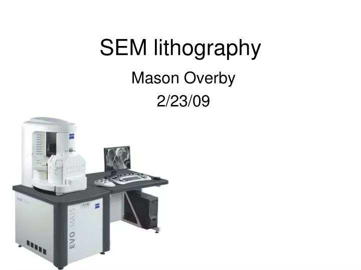
SEM lithography. Mason Overby 2/23/09. Outline. SEM (Scanning Electron Microscope) basics Why use SEM lithography Basic process for nanolithography How does this apply to carbon? Few extras…. SEM basics. Filament electron source Accelerated by variable potential “scanned”

E N D
SEM lithography Mason Overby 2/23/09
Outline • SEM (Scanning Electron Microscope) basics • Why use SEM lithography • Basic process for nanolithography • How does this apply to carbon? • Few extras…
SEM basics • Filament electron source • Accelerated by variable potential • “scanned” • scattered electrons are detected http://www.purdue.edu/REM/rs/sem.htm
SEM uses • Imaging: • Material analysis • Medical http://www.smt.zeiss.com/
SEM uses • Imaging Advantages: • Depth of Field • Resolution Lishan Weng • Disadvantages: • Setup/processing time
SEM uses • Nanolithography
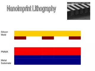
Deposited film substrate Lithography process • Clean sample • Remove oils, organics, etc (Acetone, IPA, ultrasonic) • Spin coating of photoresist on surface of film (positive or negative resist) Photoresist
Deposited film film substrate substrate film substrate Lithography process • E-beam lithography and develop • Etching • (multi-step processes) • Evaporate metal contacts film substrate
SEM uses • Imaging: After Before
substrate Lithography processfor Graphene/CNT • E-beam lithography • Evaporate metal contacts • Is it this easy? Graphene/CNT substrate
Lithography processfor Graphene/CNT • Should be the same?
Where’s the Graphene/CNT? • First must locate using optical microscope • Determine position relative to alignment marks (-a,b) (a,b) 50um (0,0) (a,-b) (-a,-b)
Where’s the Graphene/CNT? (-a’,b’) • Adjust “standard” pattern to the graphene position • Proceed as before (0’,0’)
Focusing • Fine focusing: • “burn” spot ~30-45 seconds • Focus • Check beam shape (stigmation)