Download
1 / 16
180 likes | 359 Views
Extreme Ultra-Violet Lithography. Matt Smith Penn State University EE 518, Spring 2006 Instructor: Dr. J. Ruzyllo. Outline. Why do we need EUV lithography? Brief overview of current technology What exactly is EUV? System diagram Challenges associated with EUV 13.5nm source

E N D
Extreme Ultra-Violet Lithography Matt Smith Penn State University EE 518, Spring 2006 Instructor: Dr. J. Ruzyllo
Outline • Why do we need EUV lithography? • Brief overview of current technology • What exactly is EUV? • System diagram • Challenges associated with EUV • 13.5nm source • Optics • Masks • Resists
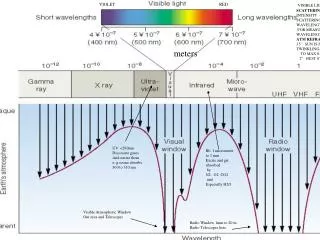
Why EUV? k1*λ NA There are only so many “tricks” to increase this gap, and they are very expensive … we MUST go to a shorter wavelength! Minimum lithographic feature size = k1: “Process complexity factor” – includes “tricks” like phase-shift masks λ: Exposure wavelength NA: Numerical aperture of the lens – maximum of 1 in air, a little higher in immersion lithography (Higher NA means smaller depth of focus, though) Mask Maker’s Holiday: “large” k1 Mask Maker’s Burden: “small” k1 ftp://download.intel.com/research/silicon/EUV_Press_Foils_080204.pdf
Mask Maker’s Holiday: “large” k1 Mask Maker’s Burden: “small” k1 Why EUV? Why not the next excimer line? • Hg (G line) @ 436nm Hg (H line) @ 405nm Hg (I line) @ 365nm • KrF Excimer @ 248nm ArF Excimer @ 193nm ??? • 157nm lithography based on the fluorine excimer laser has been largely shelved, which leaves 193nm with extensions for production • Below that, no laser line has the required output power • Excimer-based steppers expose 109 steps per 300mm wafer, and produce >100 wafers per hour – exposure times ~ 10-20ns • Additionally, fused silica and atmospheric oxygen become absorptive by 157nm – so even incremental decreases in wavelength start to require a major system overhaul ftp://download.intel.com/research/silicon/EUV_Press_Foils_080204.pdf
Why EUV? It’s all about the money. • By decreasing λ by a factor of 14, we take pressure off k1 – this makes the masks less complicated and expensive because we can skip the “tricks” • For example: a 90nm node mask set: • Pixels: • Number of pixels on 1 mask: 1012 • Defects: • Size that must be found and repaired: 100nm (25nm as projected on wafer) • Number of such defects allowed: 0 • Data: • Total file size needed for all 22-25 layers: 200GB • Cost: • Cost for mask set (depreciation, labor, etc): ~$800k-1.3M ftp://download.intel.com/technology/silicon/Chuck Gwyn Photomask Japan 0503.pdf
Current Lithographic Technology Reticle (Mask) Wafer 193 nm Excimer Laser Source Exposure Column (Lens) Computer Console • Lenses are very effective and perfectly transparent for 193nm and above, so many are used • A single “lens” may be up to 60 fused silica surfaces • System maintained at atmospheric pressure • Lens NA ~0.5-0.85 • Up to 1.1 for immersion • Exposure field 26x32mm • Steppers capable of >100 • 300mm wafers per hour • at >100 exposures per • wafer www.tnlc.ncsu.edu/information/ceremony/lithography.ppt
Basic Technology for EUV All solids, liquids, and gasses absorb 13.5nm – so system is under vacuum Mask must be reflective and exceptionally defect-free 13.5nm photons generated by plasma source All-reflective optics (all lens materials are opaque) ftp://download.intel.com/technology/silicon/EUV_Press_Foils_080204.pdf (both images)
13.5nm Plasma Radiation Source Argon Tin • The only viable source for 13.5nm photons is a plasma • Powerful plasma required – temperature of up to 200,000oC, atoms ionized up to +20 state • Plasma must be pulsed – pulse length in pico- to nanosecond range • Pre-ionized plasma excited by powerful IR laser or electric arc of up to 60,000 A to cause emission http://www.sematech.org/resources/litho/meetings/euvl/20021014/16-Spectro.pdf
Plasma Compositions for 13.5nm Argon Tin • Argon • 13.5nm photons only generated by one ion stage (Xe11+) • Even this stage emits 10 times more at 10.8nm than 13.5 • Maximum population of this stage is 45% • On the plus side, Argon is very clean and easy to work with • Argon is horribly inefficient: to produce 100W at 13.5nm, kilowatts of other wavelengths would have to be removed • Tin • Optimum emission when tin is a low-percentage impurity • All ion stages from Sn8+ to Sn13+ can contribute • Tin tends to condense on optics • Tin is great as a 13.5nm source, if we can engineer a way to use it without destroying our optics http://www.sematech.org/resources/litho/meetings/euvl/20021014/16-Spectro.pdf
Where Plasma and Optics Meet • Ions in the source plasma have enough energy to sputter material off the lenses of the collector optics • If the source uses tin, that will deposit on the lenses as well • At the power levels required for real exposures, • collector optics have a lifetime of about a month • This is VERY bad for Cost of Ownership (CoO) ftp://download.intel.com/technology/silicon/EUV_Press_Foils_080204.pdf
All-Reflective Optics • All solids, liquids, and gasses absorb 13.5nm photons • So fused silica lenses are OUT … • Indeed, all refracting lenses are OUT • Making EUV mirrors is no cakewalk, either … • 50 or more alternating Mo/Si layers give the mirror its reflectivity • Each layer is 6.7nm thick and requires atomic precision • Since the angle of incidence changes across the mirror, so do the required Mo/Si layer thicknesses • Acceptable surface roughness: 0.2nm RMS • Aspheric • Net reflectance: ~70% http://www.zeiss.com/C1256A770030BCE0/WebViewAllE/D6279194C2955B2EC12570CF0044E537
Optics System - Exposure Field Full field: ~109 exposures per 300mm wafer Development-size field: > 500,000 exposures per 300mm wafer • In July 2005, Carl Zeiss shipped the first 0.25NA full-field optics system to ASML for integration in an EUV system • Press release: http://www.zeiss.com/C1256A770030BCE0/WebViewAllE/D6279194C2955B2EC12570CF0044E537 ftp://download.intel.com/research/library/IR-TR-2003-39-ChuckGwynPhotomaskJapan0503.pdf
EUV Masks ftp://download.intel.com/research/library/IR-TR-2003-39-ChuckGwynPhotomaskJapan0503.pdf
EUV Masks NO defects are ever allowed in a completed mask • Extremely flat and defect-free substrate, perfected by smoothing layer • All defects in multilayer reflecting stack must be completely repaired • No defects allowed in absorber layer • All defects in final absorber pattern must be completely repaired • (No wonder mask sets are so expensive!) ftp://download.intel.com/research/library/IR-TR-2003-39-ChuckGwynPhotomaskJapan0503.pdf
EUV Resists Best Positive Resist 2.3mJ/cm2 LER=7.2nm Best Negative Resist 3.2mJ/cm2 LER=7.6nm LER – Line Edge Roughness 39nm 3:1 (space:line) ftp://download.intel.com/research/library/IR-TR-2003-39-ChuckGwynPhotomaskJapan0503.pdf
Conclusion • Will 193nm ever die? • As recently as 2003, EUV was “the only viable solution” for the 45nm node • Now Intel wants EUV for the 32nm node, but it may be pushed back more: • “In a nutshell, many believe that EUV will NOT be ready for the 32-nm node in 2009. Some say the technology will get pushed out at the 22- nm node in 2011. Some even speculate that EUV will never work.” • - EE Times, Jan 19, 2006 • My opinion: never say “never” about this industry… • A lot of work remains: increase output power of 13.5nm source, increase NA of reflective lenses, increase lifetime of collector optics (decrease cost of ownership) • But the potential payoff is sufficient that we will make it work