Download
1 / 81
810 likes | 1.01k Views
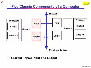
Csci 211 Computer System Architecture – Datapath and Control Design – Appendixes A & B. Xiuzhen Cheng cheng@gwu.edu. Outline. Single Cycle Datapath and Control Design Pipelined Datapath and Control Design. Processor. Input. Control. Memory. Datapath. Output. The Big Picture.

E N D
Csci 211 Computer System Architecture – Datapath and Control Design – Appendixes A & B Xiuzhen Cheng cheng@gwu.edu
Outline • Single Cycle Datapath and Control Design • Pipelined Datapath and Control Design
Processor Input Control Memory Datapath Output The Big Picture • The Five Classic Components of a Computer • Performance of a machine is determined by: • Instruction count; Clock cycle time; Clock cycles per instruction • Processor design (datapath and control) will determine: • Clock cycle time; Clock cycles per instruction • Who will determine Instruction Count? • Compiler, ISA
How to Design a Processor: Step by Step • Analyze instruction set => datapath requirements • the meaning of each instruction is given by the register transfers • datapath must include storage element for registers • datapath must support each register transfer • Select the set of datapath components and establish clocking methodology • Assemblethe datapath meeting the requirements • Analyze the implementation of each instruction to determine the settings of the control points that effects the register transfer • Assemble the control logic --- Use MIPS ISA to illustrate these five steps!
Example: MIPS r0 r1 ° ° ° r31 0 Programmable storage 2^32 x bytes 31 x 32-bit GPRs (R0=0) 32 x 32-bit FP regs (paired DP) HI, LO, PC Data types ? Format ? Addressing Modes? Memory Addressing? PC lo hi • Arithmetic logical • Add, AddU, Sub, SubU, And, Or, Xor, Nor, SLT, SLTU, • AddI, AddIU, SLTI, SLTIU, AndI, OrI, XorI, LUI • SLL, SRL, SRA, SLLV, SRLV, SRAV • Memory Access • LB, LBU, LH, LHU, LW, LWL,LWR • SB, SH, SW, SWL, SWR • Control • J, JAL, JR, JALR • BEq, BNE, BLEZ,BGTZ,BLTZ,BGEZ,BLTZAL,BGEZAL 32-bit instructions on word boundary
31 26 21 16 11 6 0 op rs rt rd shamt funct 6 bits 5 bits 5 bits 5 bits 5 bits 6 bits 31 26 21 16 0 immediate op rs rt 6 bits 5 bits 5 bits 16 bits 31 26 0 op target address 6 bits 26 bits MIPS Instruction Format • All MIPS instructions are 32 bits long. 3 formats: • R-type • I-type • J-type • The different fields are: • op: operation (“opcode”) of the instruction • rs, rt, rd: the source and destination register specifiers • shamt: shift amount • funct: selects the variant of the operation in the “op” field • address / immediate: address offset or immediate value • target address: target address of jump instruction
Name Fields Comments Field size 6 bits 5 bits 5 bits 5 bits 5 bits 6 bits All MIPS instructions 32 bits R-format op rs rt rd shamt funct Arithmetic instruction format I-format op rs rt address/immediate Transfer, branch, imm. format J-format op target address Jump instruction format MIPS Instruction Formats Summary • Minimum number of instructions required • Information flow: load/store • Logic operations: logic and/or/not, shift • Arithmetic operations: addition, subtraction, etc. • Branch operations: • Instructions have different number of operands: 1, 2, 3 • 32 bits representing a single instruction • Disassembly is simple and starts by decoding opcode field.
MIPS Addressing Modes • Register addressing • Operand is stored in a register. R-Type • Base or displacement addressing • Operand at the memory location specified by a register value plus a displacement given in the instruction. I-Type • Eg: lw, $t0, 25($s0) • Immediate addressing • Operand is a constant within the instruction itself. I-Type • PC-relative addressing • The address is the sum of the PC and a constant in the instruction. I-Type • Eg: beq $t2, $t3, 25 # if ($t2==$t3), goto PC+4+100 • Pseudodirect addressing • The 26-bit constant is logically shifted left 2 positions to get 28 bits. Then the upper 4 bits of PC+4 is concatenated with this 28 bits to get the new PC address. J-type, e. g., j 2500
MIPS Instruction Subset Core inst Register Transfers ADDU R[rd] <– R[rs] + R[rt]; PC <– PC + 4 SUBU R[rd] <– R[rs] – R[rt]; PC <– PC + 4 ORi R[rt] <– R[rs] | zero_ext(Imm16); PC <– PC + 4 LOAD R[rt] <– MEM[ R[rs] + sign_ext(Imm16)]; PC <– PC + 4 STORE MEM[ R[rs] + sign_ext(Imm16) ] <– R[rt]; PC <– PC + 4 BEQ if ( R[rs] == R[rt] ) then PC <– PC + 4 + ([sign_ext(Imm16)]<<2) else PC <– PC + 4 • ADD and SUB • addu rd, rs, rt • subu rd, rs, rt • OR Immediate: • ori rt, rs, imm16 • LOAD and STORE Word • lw rt, rs, imm16 • sw rt, rs, imm16 • BRANCH: • beq rs, rt, imm16
Step 1: Requirements of the Instruction Set • Memory • instruction & data: instruction=MEM[PC] • Registers (32 x 32) • read RS; read RT; Write RT or RD • PC, what is the new PC? • Add 4 or extended immediate to PC • Extender: sign-extension or 0-extension? • Add and Sub register or extended immediate
CarryIn A 32 Sum Adder 32 B Carry 32 Select A 32 Y MUX 32 B 32 OP A 32 Result ALU 32 B 32 Step 2: Components of the Datapath
RW RA RB Write Enable 5 5 5 busA busW 32 32 32-bit Registers 32 busB Clk 32 Storage Element: Register File • Register File consists of 32 registers: • Two 32-bit output busses: busA and busB • One 32-bit input bus: busW • Register is selected by: • RA (number) selects the register to put on busA (data) • RB (number) selects the register to put on busB (data) • RW (number) selects the register to be written via busW (data) when Write Enable is high • Clock input (CLK) • The CLK input is a factor ONLY during write operation • During read operation, behaves as combinational logic: • RA or RB valid => busA or busB outputs valid after “access time.”
Write Enable Address Data In DataOut 32 32 Clk Storage Element: Idealized Memory • Memory (idealized) • One input bus: Data In • One output bus: Data Out • Memory word is selected by: • Address selects the word to put on Data Out • Write Enable = 1: address selects the memoryword to be written via the Data In bus • Clock input (CLK) • The CLK input is a factor ONLY during write operation • During read operation, behaves as a combinational logic block: • Address valid => Data Out valid after “access time.”
Step 3: Assemble DataPath meeting our requirements • Instruction Fetch • Instruction = MEM[PC] • Update PC • Read Operands and Execute Operation • Read one or two registers • Execute operation
Clk PC Next Address Logic Address Instruction Word Instruction Memory 32 Datapath for Instruction Fetch • Fetch the Instruction: mem[PC] • Update the program counter: • Sequential Code: PC <- PC + 4 • Branch and Jump: PC <- “something else”
31 26 21 16 11 6 0 op rs rt rd shamt funct 6 bits 5 bits 5 bits 5 bits 5 bits 6 bits Datapath for R-Type Instructions • R[rd] <- R[rs] op R[rt] Example: addU rd, rs, rt • Ra, Rb, and Rw come from instruction’s rs, rt, and rd fields • ALUctr and RegWr: control logic after decoding the instruction Rd Rs Rt ALUctr RegWr 5 5 5 busA Rw Ra Rb busW 32 Result 32 32-bit Registers ALU 32 32 busB Clk 32
11 31 26 21 16 0 op rs rt immediate 6 bits 5 bits 5 bits 16 bits rd? 31 16 15 0 immediate 0 0 0 0 0 0 0 0 0 0 0 0 0 0 0 0 16 bits 16 bits Logic Operations with Immediate R[rt] <- R[rs] op ZeroExt[imm16] ] Eg. Ori $7, $8, 0x20 Rd Rt RegDst Mux Rt? Rs ALUctr RegWr 5 5 5 busA Rw Ra Rb busW 32 Result 32 32-bit Registers ALU 32 32 busB Clk 32 Mux ZeroExt imm16 32 16 ALUSrc
11 31 26 21 16 0 op rs rt immediate 6 bits 5 bits 16 bits 5 bits rd Load Operations • R[rt] <- Mem[R[rs] + SignExt[imm16]] Example: lw rt, rs, imm16 Rd Rt RegDst Mux Rt? Rs ALUctr RegWr 5 5 5 busA W_Src Rw Ra Rb busW 32 32 32-bit Registers ALU 32 32 busB Clk MemWr Mux 32 Mux WrEn Adr Data In 32 ?? Data Memory Extender 32 imm16 32 16 Clk ALUSrc ExtOp
31 26 21 16 0 op rs rt immediate 6 bits 5 bits 5 bits 16 bits Store Operations • Mem[ R[rs] + SignExt[imm16] <- R[rt] ] Example: sw rt, rs, imm16 Rd Rt ALUctr MemWr W_Src RegDst Mux Rs Rt RegWr 5 5 5 busA Rw Ra Rb busW 32 32 32-bit Registers ALU 32 32 busB Clk 32 Mux Mux WrEn Adr Data In 32 32 Data Memory Extender imm16 32 16 Clk ALUSrc ExtOp
31 26 21 16 0 op rs rt immediate 6 bits 5 bits 5 bits 16 bits The Branch Instruction • beq rs, rt, imm16 • mem[PC] Fetch the instruction from memory • Equal <- R[rs] == R[rt] Calculate the branch condition • if (Equal) Calculate the next instruction’s address • PC <- PC + 4 + ( SignExt(imm16) x 4 ) • else • PC <- PC + 4
31 26 21 16 0 op rs rt immediate 6 bits 5 bits 5 bits 16 bits 4 Adder Mux PC Adder Clk Datapath for Branch Operations • beq rs, rt, imm16 Datapath generates condition (equal) Inst Address Cond nPC_sel Rs Rt RegWr 5 5 5 busA 32 Rw Ra Rb 00 busW 32 32 32-bit Registers Equal? busB Clk 32 imm16 PC Ext
Inst Memory Adr Adder Mux Adder Putting it All Together: A Single Cycle Datapath Instruction<31:0> <0:15> <21:25> <16:20> <11:15> Rs Rt Rd Imm16 RegDst nPC_sel ALUctr MemWr MemtoReg Equal Rt Rd 0 1 Rs Rt 4 RegWr 5 5 5 busA Rw Ra Rb = busW 00 32 32 32-bit Registers ALU 0 32 busB 32 0 PC 32 Mux Mux Clk 32 WrEn Adr 1 1 Data In Extender Data Memory imm16 PC Ext 32 Clk 16 imm16 Clk ExtOp ALUSrc
Step 4: Given Datapath: RTL -> Control Instruction<31:0> Inst Memory <21:25> <21:25> <16:20> <11:15> <0:15> Adr Op Fun Rt Rs Rd Imm16 Control ALUctr MemWr MemtoReg ALUSrc RegWr RegDst ExtOp Equal nPC_sel DATA PATH
Inst Memory Adr nPC_sel 4 Adder 00 Mux PC Adder Clk imm16 PC Ext Meaning of the Control Signals • Rs, Rt, Rd and Imed16 hardwired into datapath • nPC_sel: 0 => PC <– PC + 4; 1 => PC <– PC + 4 + SignExt(Im16) || 00
Meaning of the Control Signals • MemWr: write memory • MemtoReg: 1 => Mem • RegDst: 0 => “rt”; 1 => “rd” • RegWr: write dest register • ExtOp: “zero”, “sign” • ALUsrc: 0 => regB; 1 => immed • ALUctr: “add”, “sub”, “or” RegDst ALUctr MemWr MemtoReg Equal Rt Rd 0 1 Rs Rt RegWr 5 5 5 busA = Rw Ra Rb busW 32 32 32-bit Registers ALU 0 32 busB 32 0 32 Mux Mux Clk 32 WrEn Adr 1 1 Data In Data Memory Extender imm16 32 16 Clk ExtOp ALUSrc
ALU Control and the Central Control • Two-level design to ease the job • ALU Control generates the 4 control lines for ALU operation • Func code field is only effective for R-type instructions, whose Opcode field contains 0s. • The operation of I-type and J-type instructions is determined only by the 6 bit Opcode field. • Lw/sw and beq need ALU even though they are I-type instructions. • Three cases: address computation for lw/sw, comparison for beq, and R-Type; needs two control lines from the main control unit: ALUOp: 00 for lw/sw, 01 for beq, 10 for R-type • Design ALU control • Input: the 6 bit func code field for R-type • Input: the 2 bit ALUOp from the main control unit. • Design the main control unit • Input: the 6 bit Opcode field.
ALU PC Clk An Abstract View of the Critical Path • Register file and ideal memory: • The CLK input is a factor ONLY during write operation • During read operation, behave as combinational logic: Ideal Instruction Memory Instruction Rd Rs Rt Imm 5 5 5 16 Instruction Address A Data Address 32 Rw Ra Rb 32 Ideal Data Memory 32 32 32-bit Registers Next Address Data In B Clk Clk 32
ALU PC Clk An Abstract View of the Implementation Control Ideal Instruction Memory Control Signals Conditions Instruction Rd Rs Rt 5 5 5 Instruction Address A Data Address Data Out 32 Rw Ra Rb 32 Ideal Data Memory 32 32 32-bit Registers Next Address Data In B Clk Clk 32 Datapath
Performance of Single-Cycle Datapath • Time needs by functional units: • Memory units: 200 ps • ALU and adders: 100 ps • Register file (r/w): 50 ps • No delay for other units • Two single cycle datapath implementations • Clock cycle time is the same for all instructions • Variable clock cycle time per instruction • Instruction mix: 25% loads, 10% stores, 45% ALU, 15% branches, and 5% jumps • Compare the performance of R-type, lw, sw, branch, and j
Performance of Single-Cycle Datapath • Time needed per instruction: • Variable clock cycle time datapath: R: 400ps, lw: 600ps, sw: 550ps, branch: 350, j: 200 • Same clock cycle time datapath: 600ps • Average time needed per instruction • With a variable clock: 447.5ps • With the same clock: 600ps • Performance ratio: • 600/447.5 = 1.34
Remarks on Single Cycle Datapath • Single Cycle Datapath ensures the execution of any instruction within one clock cycle • Functional units must be duplicated if used multiple times by one instruction. E.g. ALU. Why? • Functional units can be shared if used by different instructions • Single cycle datapath is not efficient in time • Clock Cycle time is determined by the instruction taking the longest time. Eg. lw in MIPS • Variable clock cycle time is too complicated. • Multiple clock cycles per instruction • Pipelining
Summary • 5 steps to design a processor • 1. Analyze instruction set => datapath requirements • 2. Select set of datapath components & establish clock methodology • 3. Assemble datapath meeting the requirements • 4. Analyze implementation of each instruction to determine setting of control points that affects the register transfer • 5. Assemble the control logic • MIPS makes it easier • Instructions same size • Source registers always in same place • Immediates same size, location • Operations always on registers/immediates • Single cycle datapath => CPI=1, CCT => long
Outline • Single Cycle Datapath and Control Design • Pipelined Datapath and Control Design
Pipelining • Pipelining is an implementation technique in which multiple instructions are overlapped in execution • Subset of MIPS instructions: • lw, sw, and, or, add, sub, slt, beq
A B C D Pipelining is Natural! • Laundry Example • Ann, Brian, Cathy, Dave each have one load of clothes to wash, dry, and fold • Washer takes 30 minutes • Dryer takes 40 minutes • “Folder” takes 20 minutes
A B C D Sequential Laundry 6 PM Midnight 7 8 9 11 10 • Sequential laundry takes 6 hours for 4 loads • If they learned pipelining, how long would laundry take? Time 30 40 20 30 40 20 30 40 20 30 40 20 T a s k O r d e r
30 40 40 40 40 20 A B C D Pipelined Laundry: Start work ASAP 6 PM Midnight 7 8 9 11 10 • Pipelined laundry takes 3.5 hours for 4 loads Time T a s k O r d e r
30 40 40 40 40 20 A B C D Pipelining Lessons 6 PM 7 8 9 • Pipelining doesn’t help latency of single task, it helps throughput of entire workload • Pipeline rate is limited by slowest pipeline stage • Multiple tasks operating simultaneously using different resources • Potential speedup = Numberpipeline stages • Unbalanced lengths of pipeline stages reduces speedup • Time to “fill” pipeline and time to “drain” it reduces speedup • Stall for Dependencies Time T a s k O r d e r
Ifetch Reg/Dec Exec Mem Wr The Five Stages of Load Cycle 1 Cycle 2 Cycle 3 Cycle 4 Cycle 5 • Ifetch: Instruction Fetch • Fetch the instruction from the Instruction Memory • Reg/Dec: Registers Fetch and Instruction Decode • Exec: Calculate the memory address • Mem: Read the data from the Data Memory • Wr: Write the data back to the register file Load
Pipelining • Improve performance by increasing throughput Ideal speedup is number of stages in the pipeline. Do we achieve this? NO! The computer pipeline stage time are limited by the slowest resource, either the ALU operation, or the memory access Fill and drain time
Ifetch Reg Exec Mem Wr Ifetch Reg Exec Mem Ifetch Ifetch Reg Exec Mem Wr Ifetch Reg Exec Mem Wr Ifetch Reg Exec Mem Wr Single Cycle, Multiple Cycle, vs. Pipeline Cycle 1 Cycle 2 Clk Single Cycle Implementation: Load Store Waste Cycle 1 Cycle 2 Cycle 3 Cycle 4 Cycle 5 Cycle 6 Cycle 7 Cycle 8 Cycle 9 Cycle 10 Clk Multiple Cycle Implementation: Load Store R-type Pipeline Implementation: Load Store R-type