Download
1 / 21
210 likes | 293 Views
Novel sensor technologies for tracking and vertexing :. A 2D position sensitive microstrip sensor with charge division. Esteban Currás Instituto de Física de Cantabria(CSIC- UC ). A segmented p-type sensor with low-gain charge amplification. Outline. Motivations for the R&D.

E N D
Novel sensor technologies for tracking and vertexing: A 2D position sensitive microstripsensor with charge division. Esteban Currás Instituto de Física de Cantabria(CSIC-UC) A segmented p-type sensor with low-gain charge amplification.
Outline • Motivations for the R&D. • A 2D position sensitive microstrip sensor. • Laser characterization • Electrical equivalent circuit simulations • Test beam results • Segmented p-type sensors with low-gain charge amplification • TCAD simulations of the device. • Laser characterization of diodes with amplification. • Conclusions E. Currás - LC Workshop 27-31 May 2013, DESY
R&DMotivation • Charge division in microstrips: • Long microstrips ladders (several tens of centimeters) proposed for the ILC tracking detectors. • Getting the particle hit coordinate along the strip using the charge division method. • Avoid the complexity of double sided sensors and the additional material of a second layer of sensors. • Low gain segmented p-type pixels (strips) • Implementing a small gain in the segmented diode so we can reduce the thickness of the sensors without reducing the signal amplitude • Smaller contribution to the material budget. E. Currás - LC Workshop 27-31 May 2013, DESY
S1 S1 with resistive coupling electrodes. Y-coordinate: Resistive charge division method. Resistive material Aluminium Aluminium y x x ** Electrode resistance >> preamplifier impedance. L L y A2 L A1+A2 S1=f(y) S2=f(L-y) = Resistive material: high doped polysilicon ** V. Radeka, IEEE Transaction on Nuclear Science NS-21 (1974) 51 S2 ChargeDivision in uStrips Simple single-side AC-coupled microstrip detectors X-coordinate: cluster-finding algorithms for strip detectors. E. Currás - LC Workshop 27-31 May 2013, DESY
Proof-of-Concept Prototype 2 Beetle chips ALIBAVA DAQ system for microstrip detectors, based on the Beetle analogue readout ASIC 3D axis stage with displacement accuracy ≈ 10 μm • Pulsed DFB laser λ=1060nm • Gaussian beam spot width ≈ 15 μm • pulse duration 2ns • 256 channels • peaking time = 25ns • S/N≈20 for standard no irradiated detectors Clean room laboratory at IFCA, Santander E. Currás - LC Workshop 27-31 May 2013, DESY
EquivalentElectricalCircuit Detector (p+-on-n) model *** 80 cells 250 μm long p e- h+ Vbias Peaking time 25ns (Beetle chip ALIBAVA DAQ system). • rise time 2ns • Q~4fC E. Currás - LC Workshop 27-31 May 2013, DESY
S1 S2 Particle t t t2 t1 V SignalPropagation– Linearity (Simulation) S1 2 mm y S2 18 mm E. Currás - LC Workshop 27-31 May 2013, DESY
R/l=2.8 Ω/μm R/l=12.2 Ω/μm 20000 events ∀ measurement Systematic error => Ballistic deficit E. Currás - LC Workshop 27-31 May 2013, DESY
A2 A1+A2 R/l=2.8 Ω/μm R/l=12.2 Ω/μm Longitudinal spatial resolution for 6 MIPs signal 1.1% L => 220 μm 1.2% L => 240 μm σA1=1.83 ADU σA2=1.80 ADU E. Currás - LC Workshop 27-31 May 2013, DESY
Test Beam Characterization • Test beam at CERN SPS Pion Beam, Nov 2012 • Firstsuccessfulintegration and synchronizationwith AIDA MIMOSA pixel telescope • Prelimiraryresults: • Monitoring of beamprofile. • Currently in progress: • Efficiency and resolutionusing tracking information. E. Currás - LC Workshop 27-31 May 2013, DESY
s/n test beam vs s/n radioctivesource Resistivestrips detector Conventionalstrips detector E. Currás - LC Workshop 27-31 May 2013, DESY
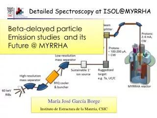
SEGMENTED P-TYPESENSORSWITHCHARGEAMPLIFICATION E. Currás - LC Workshop 27-31 May 2013, DESY
Charge Multiplication- pixel detectors We are starting the fabrication of new p-type pixel detectors with enhanced multiplication effect in the n-type electrodes, very low collection times and with no cross-talk. Three different approaches: • Thin p-type epitaxyal substrates • Low gain avalanche detectors • 3D with enhanced electric field. Two projects funded by CERN RD50 collaboration to work on these technologies. http://rd50.web.cern.ch/rd50/ E. Currás - LC Workshop 27-31 May 2013, DESY
Low gain avalanche detectors (LGAD) N+ Implating an n++/p+/p- junction along the centre of the electrodes. Under reverse bias conditions, a high electric field region is created at this localised region, which can lead to a multiplication mechanism (impact Ionization). High Electric Field region leading to multiplication Advantages = Thinning while keeping same S/N as standard detectors. P 285 um P. Fernandez et al, “Simulation of new p-type strip detectors with trench to enhance the charge multiplication effect in the n-type electrodes” , Nuclear InstrumentsandMethodsinPhysicsResearchA658(2011) 98–102. E. Currás - LC Workshop 27-31 May 2013, DESY
Simulation of the Electric Field - To obtain the manufacture parameters (doping profiles) Standard Strip Strip with P-type diffusion Strip with P-type diffusion: 2D and 1D doping profiles E. Currás - LC Workshop 27-31 May 2013, DESY
Red laser TCTcharacterization Bottominjection Standard diode n on p P-type diffusion diode 5ns 285 um h+ e- Red laser (1060 nm) E. Currás - LC Workshop 27-31 May 2013, DESY
Red laser TCT characterization Chargecollectionefficiency Standard diode P-type diffusion diode E. Currás - LC Workshop 27-31 May 2013, DESY
Mask set (planar) AC 1 Strip = 24 Metal = 20 AC 2 Strip = 24 Metal = 24 AC 3 Strip = 24 Metal = 28 AC 5 Strip = 48 Metal = 48 AC 6 Strip = 48 Metal = 52 AC Strip = 32 Metal = 40 DC Strip = 32 Metal = 40 AC 4 Strip = 48 Metal = 44 DC Strip = 32 Metal = 40 AC 8 Strip = 62 Metal = 62 AC 9 Strip = 62 Metal = 66 AC Strip = 32 Metal = 40 AC 7 Strip = 62 Metal = 58 FEI4 With Guard rings FEI4 With Guard rings FEI4 With one Guard ring FEI4 With one Guard ring FEI3 With Guard rings FEI3 With one Guard ring CMS pixel detectors FEI3 With Guard rings E. Currás - LC Workshop 27-31 May 2013, DESY
Summary • A novel 2D position-sensitive semiconductor detector concept based on the resistive charge-division readout method has been introduced. • The initial results demonstrates the feasibility of the charge division method in a fully fledged microstrip sensor. • Test-beam studies on detection of minimum ionizing particles are in progress • The effect of charge multiplication has been observed within RD50 and it was started to be investigated systematically. • New detector designs aim to fabricate detectors with moderate gain and fast collection times. E. Currás - LC Workshop 27-31 May 2013, DESY

![[1] Instituto de Ciencias del Mar, CSIC, Barcelona, España, mikhail@icm.csic.es;](https://cdn1.slideserve.com/3208993/slide1-dt.jpg)