Download
1 / 17
200 likes | 390 Views
Plasma Etching of Cesium Iodide Xiaoji Yang and Jeffrey A. Hopwood Northeastern University Boston, Massachusetts 02115 S. Tipnis, V. Nagarkar, and V. Gaysinskiy Radiation Monitoring Devices, Inc. Watertown, Massachusetts Supported by NIH Grant No. 2R44 CA76758-02.

E N D
Plasma Etching of Cesium Iodide Xiaoji Yang and Jeffrey A. Hopwood Northeastern University Boston, Massachusetts 02115 S. Tipnis, V. Nagarkar, and V. Gaysinskiy Radiation Monitoring Devices, Inc. Watertown, Massachusetts Supported by NIH Grant No. 2R44 CA76758-02
Outline • Background for X-ray imaging sensors • Project methodology • Summary of experimental results • Conclusion: Ion-enhanced inhibitor etching mechanism Electronic sputtering mechanism
Background: Pixelated Scintillators • Core glass is selectively etched from FOP • The remaining cladding forms 6 um cavities • Phosphorus grains are used to refill cavities • Using a slow sedimentation technique • Fouassier et al. (1985)
Background: Pixelated Scintillators • Cladding is selectively etched leaving only the core glass • CsI is directionally deposited on top of the core glass • Oba et al. (1987)
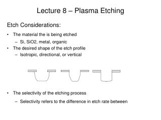
Anisotropic Plasma Etching of CsI • Deposit optimal, full-density CsI thick films • 8-70 keV x-ray conversion requires ~30 - 200 um thick CsI films • Resolution requirements dictate ~50 um pixels • Define pixel mask using a dry process • CsI is soluble in water, PR developer…almost all commonly used solvent! • Anisotropically etch CsI films into pixels
Dry etch mask fabrication Nickel mesh with adhesive TiW CsI Fiber optic plate Evaporate Al mask after Remove Ni mesh, O2 etching adhesive Plasma etch CsI Normal Conditions: 400 W ICP, 200 W bias, 3 mtorr Ar+CF4, 220 oC
Experimental Configuration I HeNe for temperature measurement time
Etch Inhibitor on Sidewalls Al mask CxFyCsz Cs:I = 6 : 1 Cs:I = 1.3 : 1 400W ICP, 200W Bias, 3 mtorr Ar+CF4, 220 oC
[F] vs. CxFyCsz polymerization Eion ~ 120 eV
Ion Bombardment Energy T=220°C I. Net deposition of inhibitor - no etching II. Inhibitor suppression - layer thickness reduced III. Reactive sputtering region - negligible inhibitor - Rate ~ Eion1/2 - Eth ~ 20 eV “Ion-enhanced inhibitor etching mechanism”
Temperature Dependence Ion energy=120 eV
Electronic Stopping “High Temp.” “Low Temp.” Halogen Vacancy/Interstitial Recombination Self-trapped Excitons Radiative Decay Diffusion to surface Luminescence Electronic Sputtering Electronic Sputtering • Electronic sputtering dominates over collision cascades in the sputtering of alkali halides • Thermal activation of CsI etching (Ea = 0.13±0.01 eV) is similar to other alkali halides. • Ea = 0.17 eV for KCl sputtered by Ar+ at 70-300 keV. (Biersack et al.) • Electronic Sputtering Mechanism: (after Szymonski, 1990)
Conclusion • Anisotropic etching to depths of 50 um. • CsI is etched by the “Ion-enhanced Inhibitor Mechanism” using CF4 + Ar plasma. • Electronic sputtering with Ea = 0.13 eV. Future Work • What is the mechanism by which F atoms increase the etch rate? (CsF is involatile)
Speculative Mechanism • F atoms do not volatilize Cs • therefore, this is probably not a classic chemical etch • F atoms can diffuse into the heated CsI surface • Interaction of F with excitons impedes radiative recombination and enhances electronic sputtering