Download
1 / 8
80 likes | 228 Views
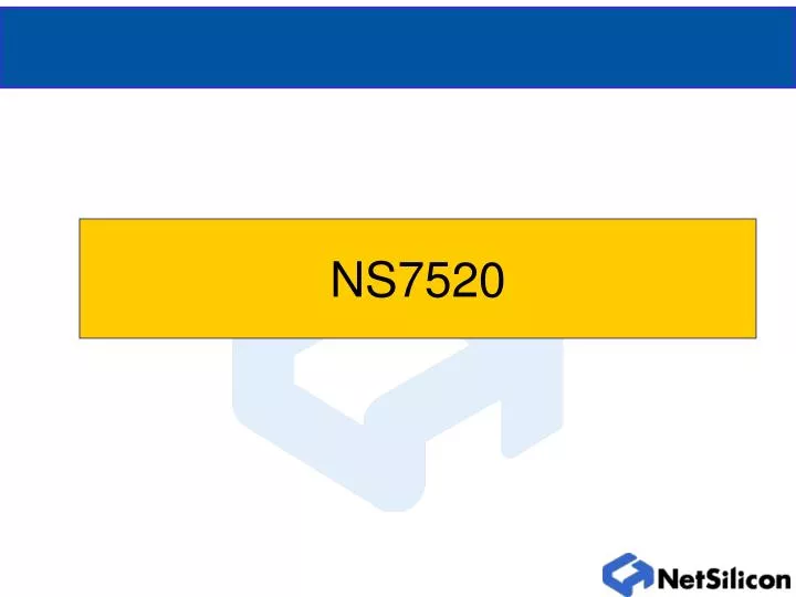
NS7520. NS7520. 177 Pin Plastic BGA. ARM. NS7520 Block Diagram. Block Diagram. JTAG - Boundary Scan. ARM7TDMI. ARM7TDMI. GP I/O. 32-Bit RISC Architecture Load-Store Architecture Fixed Length 32-bit Instructions 3-address Instruction Format 2 Instruction Sets (Standard & Thumb)

E N D
NS7520 177 Pin Plastic BGA
ARM NS7520 Block Diagram Block Diagram JTAG - Boundary Scan ARM7TDMI ARM7TDMI GP I/O • 32-Bit RISC Architecture • Load-Store ArchitectureFixed Length 32-bit Instructions3-address Instruction Format • 2 Instruction Sets (Standard & Thumb) • 3-Stage Pipeline • 13 / 8 universal 32-Bit Registers • 32 Bit PC und SR • 50 MIPS (Peak) • 5 Supervisor-, 1 User-Mode • Big- und Little-Endian Format • Memory Mapped I/O 4 x INT 16 x I/O BBus 2 x Serial JTAG - Boundary Scan JTAG - Boundary Scan 10-Channnel DMA BBus 10/100 Ethernet MAC Timers WD EBI Mem. Contr. CS-Unit Clock JTAG - Boundary Scan
NS7520 Overview • No Cache • No Port B • No Parallel Ports, No ENI • Less GPIO, only Port A and Port C • Register address changes in Ethernet module • Some bits changes in eth & spi registers
NS7520… • The newest NET+ARM family member, packaged in a 13x13mm package with 177 balls, (One of which is a locator). • The NS7520 (due to the .18- micron process technology used) has a lower core voltage (1.5V). • The NS7520 utilizes special I/O cells that can continue to be powered at 3.3V. This feature allows the NET+ARM family to continue its long tradition of interfacing with 3V LVTTL technology. • The NS7520 will operate from the same 18.432MHZ crystal, or external oscillator up to 55MHz. 2.5V should power the external oscillator, or a 3.3V oscillator can be used with a voltage divider to reduce its output to a 2.5V signal level.
Added Features • Three Additional DMA Channels, plus 13 USB (device) DMA channels • Up to 55MHz System Clock (NET+20M up to 44MHz) • 512 Byte Ethernet Transmit Buffer (NET+20M has 128 byte) • Supports JTAG Boundary Scan in addition to JTAG debug • Smaller BGA Package • USB V1.1 (Configurable as Device)
The ARM7TDMI Core The ARM7TDMI is a well established core in the industry. The TDMI portion stands for T Thumb Mode – A 16-bit instruction set D Debugger Module – A module that allows halting of the core and inserting instructions M Multiply – This version of the core supports a special multiply set of instructions which can yield 64 bit results I Ice Breaker Module – The ICE breaker supports the use of two hardware breakpoints
ARM7TDMI Block Diagram scan chain 2 scan chain 0 Embedded ICE Processor Core other Signals opc, r/w, mreq, trans, mas[0:1] A[31:0] D[31:0] scan chain 1 JTAG TAP Controller Bus Splitter Din[31:0] scan chain 3 Dout[31:0] TRST TDI TCK TMS TDO