Download
1 / 32
320 likes | 334 Views
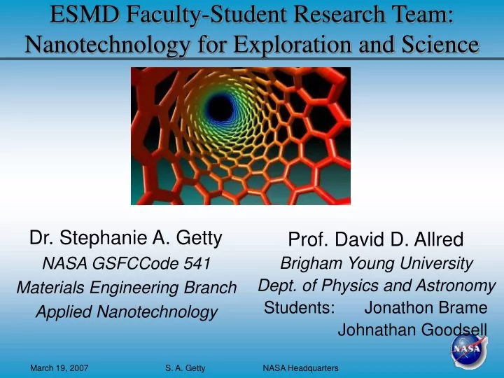
ESMD Faculty-Student Research Team: Nanotechnology for Exploration and Science. Dr. Stephanie A. Getty NASA GSFCCode 541 Materials Engineering Branch Applied Nanotechnology. Prof. David D. Allred Brigham Young University Dept. of Physics and Astronomy Students: Jonathon Brame

E N D
ESMD Faculty-Student Research Team: Nanotechnology for Exploration and Science Dr. Stephanie A. Getty NASA GSFCCode 541 Materials Engineering Branch Applied Nanotechnology Prof. David D. Allred Brigham Young University Dept. of Physics and Astronomy Students: Jonathon Brame Johnathan Goodsell S. A. Getty NASA Headquarters
NASA’s Exploration Initiative Courtesy NASA website To the Moon, Mars and BeyondThe Vision for Space Exploration calls for humans to return to the moon by the end of the next decade, paving the way for eventual journeys to Mars and beyond. Carbon Nanotube- Magnetic analysis of geological based Magnetometer : samples on Mars and the Moon Orientation for manned expeditions Location of mining resources Courtesy NASA website To the Moon, Mars and BeyondThe Vision for Space Exploration calls for humans to return to the moon by the end of the next decade, paving the way for eventual journeys to Mars and beyond. S. A. Getty NASA Headquarters
Projects ongoing in GSFC NanoDevices Group • Strain-based NanoCompass • GSFC: 541, 691 • BYU summer intern team: Prof. D. Allred, Johnathan Goodsell, Jon Brame • Electron gun for miniaturized mass spectrometer • GSFC: 541, 553, 699 • Fisk University summer intern: Melissa Harrison • Generalized strain sensors • GSFC: 541, 660 • BYU summer intern team: Prof. D. Allred, Johnathan Goodsell, Jon Brame • Fisk University summer intern: Melissa Harrison S. A. Getty NASA Headquarters
Background Information:Carbon Nanotubes S. A. Getty NASA Headquarters
Nanoelectronic Materials Single-walled Carbon Nanotubes • Metallic or Semiconducting • Difficult to control trend toward SWCNT network devices • Electronic properties sensitive to deformation • Strain sensing Courtesy Smalley Group, Rice Univ. S. A. Getty NASA Headquarters
Vapor-Liquid-Solid Growth Feedstock gas liquid alloy solid nanostructure • SWCNTs: • Catalyst = Fe(NO3)3:IPA or thin film Fe • Feedstock = CH4 and C2H4 • TG = 950°C, tG = 5-10 minutes • MWCNTs: • Catalyst = thin film Al/Fe bilayer • Feedstock = C2H4 • TG = 750°C, tG = 5-10 minutes S. A. Getty NASA Headquarters
NanoCompass Thin Film Fe Catalyst • High density • Improved cleanliness TG = 950°C • TEM studies show • SWCNTs • MWCNTs • bundles Johnathan Goodsell, Prof. David Allred, Prof. R. Vanfleet (BYU) S. A. Getty NASA Headquarters
Johnathan Goodsell Brigham Young University Mechanical Engineering Major Summer project: Optimize growth of SWCNTs using thin film catalyst New process for GSFC Crucial for NanoCompass development Excellent results in only 8 weeks Contributed to IEEE Nano 2006 Presentation, Cincinnati, OH, July 2006 Summary of Progress: SWCNT Growth S. A. Getty NASA Headquarters
SWCNT NanoCompass for High Spatial Resolution Magnetometry S. A. Getty NASA Headquarters
Technological Motivation Mars Applications: • Magnetospheric Science • Spacecraft Orientation • Planetary Geomagnetism • Fluxgate Magnetometer: • High sensitivity (nTesla) • Low noise • but • cm-scale resolution • Limited materials supply M. H. Acuna, Rev. Sci. Inst. 73, 3717 (2002) S. A. Getty NASA Headquarters
NanoCompass NanoCompass Design Single-Walled Carbon Nanotubes ●Ferromagnetic Needle • Mech coupled to SWCNTs • Deflected in Magnetic Field ●Au Electrodes S. A. Getty NASA Headquarters
Projected Specifications S. A. Getty NASA Headquarters
NanoCompass NanoCompass Fabrication (to step 4) Materials can be robust to fabrication process Next steps: • Reduce electrode spacing • Reduce needle width • Increase trench depth S. A. Getty NASA Headquarters
Future Work: Variability in Processing Au SWCNTs Remnant needle Au • SWCNT device electrically intact • During magnetic field testing, continuity lost • Next prototype in progress S. A. Getty NASA Headquarters
Generalized Strain Sensing Using SWCNTs S. A. Getty NASA Headquarters
Flexible substrates • Parylene, PDMS are candidates • Modular electromechanical strain sensors • Modular field emitters • Application-adaptive devices • Parylene: vapor-phase coated polymer, highly chemically resistant, excellent electronic insulator • PDMS: polydimethylsiloxane, two-part curable elastomer, chemically resistant, good electronic insulator – to be demonstrated in SWCNTs S. A. Getty NASA Headquarters
Device Transfer to Parylene • 1. Fabricate SWCNT device • on rigid substrate to allow • electrical characterization 2. Deposit parylene O2 plasma • 3. Transfer to PDMS by substrate removal Wet etch S. A. Getty NASA Headquarters
Flexible Substrates Parylene-bound SWCNT Strain Device Jonathon Brame, Prof. David Allred (BYU) S. A. Getty NASA Headquarters
Flexible Substrates Preliminary Results The slope of the lines between 4µm stretch sets indicates that the resistance increases reversibly with increased strain. • Large increase in device resistance with application of strain, as expected • Need to separate contact effects from piezoresistive effects • Need to evaluate reproducibility S. A. Getty NASA Headquarters
Jonathon Brame Brigham Young University Physics Major Summer project: Demonstrate transfer of SWCNTs to parylene substrates Test electromechanical response Preliminary fabrication and test completed in only 12 weeks Publication and presentation at MRS Fall Meeting, Boston, November 2006 “Strain-based Electrical Properties of Systems of Carbon Nanotubes Embedded in Parylene,” Jon Brame, Stephanie Getty, Johnathan Goodsell, and David Dean Allred, Proceedings, Materials Research Society Fall 2006 Meeting. Summary of Progress: Parylene-bound SWCNT Devices S. A. Getty NASA Headquarters
BYU Team has major role in Mars Desert Research Station (UT) In situ demonstration of NanoCompass operation Student-operated for outreach effort Relevant to manned missions to the Moon and Mars Joint proposal submitted to support NanoCompass: ROSES Planetary Instrument Definition and Development Decision Pending Building growth/characterization facility at BYU Correlated results, independent of location, important to the CNT field Measurements of CNT response in extreme UV planned Possible applications in nanomaterial sensing for workplace safety monitoring Status of Collaboration: GSFC-BYU Team S. A. Getty NASA Headquarters
Acknowledgements • Dr. Peter Wasilewski GSFC/Astrochemistry Laboratory • Dr. Louis Barbier GSFC/Exploration of the Universe Division • Dr. Paul Mahaffy GSFC/Atmospheric Experiments Laboratory • Patrick Roman GSFC/Detector Systems Branch • Barney Lynch GSFC/Detector Systems Branch • Dr. Federico Herrero GSFC/Detector Systems Branch • Rusty Jones GSFC/Detector Systems Branch • Dr. Todd King GSFC/Materials Engineering Branch • Rachael Bis GSFC/Materials Engineering Branch • Michael Beamesderfer GSFC/Materials Engineering Branch • Lance Delzeit ARC/Nanotechnology Branch • Prof. Gunther Kletetschka GSFC/Catholic University of America • Vilem Mikula GSFC/Catholic University of America • Tomoko Adachi GSFC/Catholic University of America ESMD Summer Internship Program • Prof. David Allred Brigham Young University/Dept. of Physics & Astronomy • Prof. Richard Vanfleet Brigham Young University/Dept. of Physics & Astronomy • Johnathan Goodsell Brigham Young University/Mechanical Engineering Dept. • Jonathon Brame Brigham Young University/Dept. of Physics & Astronomy MUCERPI Summer Internship Program • Melissa Harrison Fisk University This work was supported by the Goddard Space Flight Center Director’s Discretionary Fund, the GSFC IRAD Program, the Minority University College Education and Research Partnership Initiative, and the Exploration Systems Mission Directorate Faculty-Student Summer Internship Program S. A. Getty NASA Headquarters
Extra Slides S. A. Getty NASA Headquarters
Nanoelectronic Materials Courtesy Fuhrer Group, Univ Maryland, College Park Single-walled Carbon Nanotubes • Characterized by chirality, diameter • Diameter ~ 1 nm • Metallic or Semiconducting • Difficult to control trend toward SWCNT network devices • Electronic properties sensitive to deformation • Strain sensing Metallic SWCNT: n – m = 3 x integer Courtesy Smalley Group, Rice Univ. S. A. Getty NASA Headquarters
Nanoelectronic Materials, Cont. Multi-walled Carbon Nanotubes • Exclusively metallic • Similar to graphite • Diameters 30-100 nm • Larger than SWCNTs • High aspect ratio with many available electrons • Field emission S. A. Getty NASA Headquarters
E-gun for MEMS Time-of-Flight Planetary Atmospheric Science Mass Spectrometer : and biologically significant molecular species for astrobiology Ion lens assembly prototype Carbon Nanotube-based Electron Gun S. A. Getty NASA Headquarters
Field Emission Comparison: Candidate Technologies MWCNTs Spindt Emitters Thermionic *This work **Optimized †V. M. Aguero and R. C. Adamo, 6th Spacecraft Charging Technology Conference (2000). ¶Barium Oxide-coated Tungsten S. A. Getty NASA Headquarters
Field Emission Patterned CNT Cathode • CNT tower dimensions • 5 μm x 5 μm x 10μm (height) • 50 μm pitch • 2mm x 2mm array S. A. Getty NASA Headquarters
Field Emission Patterned MWCNTs for High Performance E-gun GSFC patterned MWCNT emitter: • Cathode-grid spacing = 140 µm • Turn-on voltage <100 V • 50 µA @ 10 mW Compare to Cassini-Huygens thermionic e-gun: • 80 µA @ 1000 mW S. A. Getty NASA Headquarters
Field Emission Sample Database GSFC:EGp2 • Best performer: • GSFC patterned sample • 50 uA @ gap = 140 um S. A. Getty NASA Headquarters
Field Emission Side-by-Side E-Gun Evaluation lens stack filament repeller Thermionic e-gun CNT e-gun Recent and Upcoming Work: Compare candidate e-gun technologies, fully integrated with aperture/lens stack Towards Integration into MEMS Time-of-Flight Mass Spectrometer S. A. Getty NASA Headquarters
Lifetime testing of CNT emitters Study of performance in ambient gas environment Maturation of fabrication techniques Maturation of packaging techniques Advanced electronics to develop feedback/ballast for current stabilization Future Work for Summer Interns: CNT E-Gun S. A. Getty NASA Headquarters