Download

1 / 39
430 likes | 962 Views
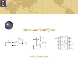
Operational Amplifiers. 1. Introduction. (The first IC op amp was introduced in mid-1960s .). Why op amp is so popular ?. We can do almost anything with op amp, such as, summation, subtraction, amplification, differentiation, integration, …. Operational Amplifier.

E N D
Introduction (The first IC op amp was introduced in mid-1960s.) Why op amp is so popular ? • We can do almost anything with op amp, such as, summation, subtraction, amplification, differentiation, integration, …. Operational Amplifier • Op amp has almost ideal characteristics. You should be able to design nontrivial circuit by the end of this chapter ! • Op amp works almost same as it is expected. What’s inside of op amp ? Chap. 9, complex but useful for high level engineer. 2.1 The Ideal Op Amp 2.1.1 The Op-Amp Terminals No terminal of op-amp package is physically connected to ground. Microelectronic Circuits - Fifth Edition Sedra/Smith
2.1.2 Function and Characteristics of the Ideal Op Amp • Op amp is a differential-input single ended-output amplifier. • Op amp is a directly-coupled or dc amplifier. - useful, but can cause some serious practical problems A: open-loop gain, differential gain 2.1.3 Differential and Common-mode Signals (How are we going to use it?) (Feedback, closed loop) Microelectronic Circuits - Fifth Edition Sedra/Smith
2.2 The Inverting Configuration Negative feedback Figure 2.5 The inverting closed-loop configuration. (Output is 180o phase-shifted w.r.t the input.) Figure 2.12 The noninverting configuration. p.77 Sect.2.3 (Output is in phase with the input.) 2.2.1 The closed-Loop Gain Ideal op amp: open loop gain A = ∞ The terminal 1and 2 are virtually shorted. The terminal 1 is a virtual ground ! The virtual ground isnot an actual ground. Do not short the inverting input to ground to simplify analysis ! Microelectronic Circuits - Fifth Edition Sedra/Smith
① Procedure to find output voltageυo. • υo will be 180o phase-shifted with respect to the input wave. Inverting amplifier ! • We can make the closed-loop gain as accurate as we want by selecting passive components of appropriate accuracy. • The closed-loop gain is (ideally) independent to the op-amp gain. Microelectronic Circuits - Fifth Edition Sedra/Smith
103 104 105 2.2.2 The Effect of Finite Open-Loop Gain (A≠∞) ① EXAMPLE2.1 p.72 υ1 Microelectronic Circuits - Fifth Edition Sedra/Smith
The production spread in the value of open-loop gainA between op-amp units of the same type (part number) is very wide. Microelectronic Circuits - Fifth Edition Sedra/Smith
R ① Contradiction ! Solution: example 2.2 2.2.3 Input and output Resistance of Inverting Amplifier (not op-amp) What would happen if R1 is too small ? Therefore, input resistance R1 should be much larger than output resistance of previous stage. Unfortunately, the internal resistance of most sensors are large. Ideal input resistance of inverting amplifier, not op-amp. For high gain (- R2 / R1), we need small R1, otherwise, R2 would be impractically large. Microelectronic Circuits - Fifth Edition Sedra/Smith
(a) Find EXAMPLE2.2p73 (b) Design the inverting amplifier with gain of 100 and an input resistance 1 MΩ. (a) (b) input resistance 1 MΩ R1=1 MΩ maximum resistance in practical circuits: 1 MΩ R2, R4=1 MΩ gain of -100 R3=10.2 k Ω (If we adopt a typical inverting amplifier and R1=1 MΩ, R2=100 MΩ, impractically large !) Microelectronic Circuits - Fifth Edition Sedra/Smith
Transresistance (transimpedance) amplifier and current amplifier • Photodiode (photodetector) generates electron-hole pairs proportional to the incident light power. • Therefore, photodiode is a current source (I). • υo = - IR2 means current input, voltage output ! Transresistance amplifier ! Figure 2.9 A current amplifier based on the circuit of Fig. 2.8. The amplifier delivers its output current to R4. It has a current gain of (1 + R2/R3), a zero input resistance, and an infinite output resistance. The load (R4), however, must be floating (i.e., neither of its two terminals can be connected to ground). • Input resistance is R2/A, very small. (Try this!) • Since the photodiode has capacitance inside, if a large resistor for high output voltage is used instead of op-amp, time constant would be large, which means it can not be used in high frequency circuit. • Transresistance amplifier is currently used as a part of receiver in high speed fiber-optic communication systems. Microelectronic Circuits - Fifth Edition Sedra/Smith
2.2.3 An Important Application-The Weighted Summer. Figure 2.10 A weighted summer. Mom, virtual grounds are extremely handy ! Figure 2.11 A weighted summer capable of implementing summing coefficients of both signs. Microelectronic Circuits - Fifth Edition Sedra/Smith
2.3 The Non-inverting Configuration 2.3.1 Theclose-Loop Gain The inverting configuration. Figure 2.12 The noninverting configuration. • the Role of Negative feedback 1. LetυI increase. Let’s derive the expression of the voltage gain. 2. υId is increased. 3. υo is increased. 4. Fraction ofυo will be fed back to (-) terminal. 5. This feedback will be counteract the increase inυId , driving back to zero. – degenerative feedback • Another derivation υo is divided to R1 and R2. Microelectronic Circuits - Fifth Edition Sedra/Smith
2.3.2 Characteristics of the noninverting Configuration - Input and output signals have same phase.-noninverting. - Input impedance is infinite. - output impedance is zero. 2.3.3 Effect of Finite Open-Loop Gain - Follow the procedure used for inverting amplifier. - non-inverting amplifier - denominators are identical ! How come? - inverting amplifier identical negative feedback (think about 0 V input !) - numerators are different ! How come? different amount of feedback (closed loop gain) In order to minimize the effect of the finite open-loop gain, Microelectronic Circuits - Fifth Edition Sedra/Smith
2.3.4 The Voltage Follower - Input impedance is infinite. - very desirable feature. - Buffer Amplifier ! to connect a source with a high impedance to a low-impedance load Usually, gain = 1 (Sect. 1.5) Why do we need this? - 100% feedback ! - Used as impedance transformer or power amplifier. - Elegant in simplicity ! The unity-gain buffer or voltage follower. equivalent circuit model. Microelectronic Circuits - Fifth Edition Sedra/Smith
2.4 Difference (differential) Amplifiers (very important application) Common mode input differential gain differential input Common mode gain≈0 • The efficacy of a differential amp is measured by the degree of its rejection of common-mode signals in preference to differential input signals. Transducer (sensor) We want to amplify the sensor output only. (we want to reject common-mode noise signal.) Noise (Electromagnetic Interference, EMI) from motor, spark, lightning… 2.4.1 A single Op-Amp Difference Amplifier Gain of the inverting amplifier = -R2/R1 Combine these two amp. Independently adjustable or matched gain Gain of the non-inverting amplifier = 1+R2/R1 Microelectronic Circuits - Fifth Edition Sedra/Smith
Figure 2.16 A difference amplifier. To make gain R2/R1, Superposition ! For easier matching, R3=R1, R4=R2 Microelectronic Circuits - Fifth Edition Sedra/Smith
Differential input Resistance Rid Drawback 1: for large gain, very small R1 is required. Drawback 2: to vary the gain, two resistances should be changed. 2.4.2 A Superior Circuit-The Instrumentation Amplifier The Goal: High differential gain with high input resistance and easy gain control HOW? Voltage follower with gain + Difference amplifier Disadvantages 1: in the first stage, common-mode gain = differential gain may causes saturation of op-amp. 2: in the first stage, two amplifiers have to be perfectly matched. 3: to vary the gain, two resistances (two R1) should be changed. There is a simple solution ! Microelectronic Circuits - Fifth Edition Sedra/Smith
Instrumentation Amplifier 1 2 6 4 5 8 7 3 9 1 Microelectronic Circuits - Fifth Edition Sedra/Smith
EXAMPLE2.3 Design The instrumentation amplifier circuit to provide a gain that can be varied over the range of 2 to 1000 utilizing a 100 kΩ variable resistance ( a potentiometer or “pot” for short). (Sol.) • It is usually preferable to obtain all the required gain in the first stage. (Low Noise) • The second stage (difference amp) is usually designed for a gain of 1. • We select all the second-stage resistors to be 10 kΩ, practically convenient value. R1f =100 Ω, 1% R1f =100.2 Ω, R2 = 49.9 kΩ, 1% R2 = 50.050 kΩ, Microelectronic Circuits - Fifth Edition Sedra/Smith
2.5 Effect of Finite Open-Loop Gain and Bandwidth on Circuit Performance A circuit designer has to be thoroughly familiar with the characteristics of practical op amps and the effects of such characteristics on the performance of op-amp circuits. 2.5.1 Frequency Dependence of the Open-Loop Gain - Internally compensated op amps are unit that have a network (usually a single capacitor) within the IC chip. - Capacitor’s function is to cause the op-amp gain to have the STC low-pass response. - This process of modifying the open-loop gain is termed to frequency compensation. - The purpose of frequency compensation is to ensure that the op-amp will be stable (as oppose to oscillation: Ch. 8). Figure 2.22 Open-loop gain of a typical general-purpose internally compensated op amp. - ft = ωt/2πis specified on the data sheet as unity-gain band width. Microelectronic Circuits - Fifth Edition Sedra/Smith
If ft is known, one can easily determine the magnitude of the op-amp gain at a given frequency when f >> fb. The production spread in the value of ftbetween op-amp units of the same type (part number) is much smaller than that of A0 and fb. ftis preferred as a specification parameter. - An op amp having this -6 dB/octave (= - 20 dB/decade) gain roll off is said to have a single-pole model. - Since this single pole dominates the amplifier frequency response, it is called a dominant pole. (for more on poles and zeros, refer to Appendix E.) 2.5.2 Frequency Dependence of the Closed-Loop Gain The effect of limited op-amp gain and bandwidth on the closed-loop transfer functions. Microelectronic Circuits - Fifth Edition Sedra/Smith
Low-Pass STC Network ! EXAMPLE2.4 ft = 1 MHz, find 3-dB frequency of closed-loop amp with gain of 1000, 100, 10, 1, -1, -10, -100, -1000 Gain-bandwidth product = 1000 V/V-kHz = 60dB-kHz Non-inverting amplifier Microelectronic Circuits - Fifth Edition Sedra/Smith
2.6 Large-signal Operation of Op Amps 2.6.1 Output Voltage Saturation Rated output voltage (output saturation voltage) = ± L (L=VDD – α V ) 2.6.2 Output Current Limits For example, maximum output current of 741 is ± 20 mA. EXAMPLE2.5 Output saturation voltage = ± 13 V, output current limits = ± 20 mA (a) Output voltage for Vp =1 V, RL= 1 kΩ υo/ υI = (1+R2/R1): Vop = 10 V, Iop = 10 mA (b) Output voltage for Vp =1.5 V, RL= 1 kΩ Vop = 15 V, Iop = 14.3 mA (c) for RL= 1 kΩ, Vpmax= ? for undistorted output. 13/10 = 1.3 V ( 14.3 mA) (d) for Vp =1.5 V, RLmin= ? for undistorted output. Microelectronic Circuits - Fifth Edition Sedra/Smith
2.6.3 Slew Rate - Another nonlinear distortion due to the large output signal Slew Rate : maximum rate of change possible at the output of a real op amp Why this happens ? : Chap. 9 SR is distinct from the finite op-amp bandwidth. - The limited bandwidth : linear, no distortion, but reduced gain at higher frequency. - The limited Slew-rate : nonlinear distortion, even at low frequency when output is too large. When V is sufficiently small, the output can be the exponentially rising ramp. This is a low-pass STC response. Output from capacitor of RC network ! Microelectronic Circuits - Fifth Edition Sedra/Smith
2.6.4 Full-Power Bandwidth Figure 2.27 Effect of slew-rate limiting on output sinusoidal waveforms. At which an output sinusoid with amplitude equal to the rated output voltage of the op amp begins to show distortion due to slew-rate limiting. 2.7 DC Imperfection 2.7.1 Offset Voltage Op amps are direct-coupled devices. They are prone to dc problems. • With inputs being zero, the amplifier output rests at some dc voltage level instead of zero. The equivalent dc input offset voltage is Microelectronic Circuits - Fifth Edition Sedra/Smith
R1 =1.2 kΩ, R2 = 1 MΩ, To include effect of offset voltage, υO = ? If υid =0, When an input signal is applied to the amplifier, the corresponding signal output will be superimposed on the 2.5 V dc. Then the allowable signal swing at the output will be reduced. If signal is dc, we would not know where the output is due to VOS or the signal. (another interpretation of CMMR) * To overcome dc offset problem • Thus, CMRR is a measure of how total offset voltage vOS changes from its dc value VOS when common-mode voltage is applied. * The gain will fall off at the low- frequency. Figure 2.28 Circuit model for an op amp with input offset voltage VOS. Microelectronic Circuits - Fifth Edition Sedra/Smith
2.7.2 Input Bias and Offset Current * To find the dc output voltage of the closed-loop amp due to the input bias current In order for the op amp to operate, its two input terminals have to be supplied with current, termed the input bias current. Why? Bias currents (base currents in BJTs or gate currents in MOSFETs or JFETs) are similar in value with directions depending on internal amplifier circuit type. How to reduce the dc output voltage due to the input bias current Microelectronic Circuits - Fifth Edition Sedra/Smith
There should be a continuous dc path between each input terminal and ground. Conclusion: To minimize the effect of the input bias current, Place in the positive lead a resistance equal to the dc resistance seen by the inverting terminal. This circuit will not work. This circuit will work. Microelectronic Circuits - Fifth Edition Sedra/Smith
* dc gain=?, 3 dB frequency=? * Design a circuit of dc gain=40 dB, 3 dB frequency=1 kHz, input resistance = 1 kΩ * Frequency of gain=1 and phase at this frequency 2.8 Integrators and Differentiators 2.8.1 The Inverting Configuration with General Impedances Example 2.6, p106 Sol) * Is this STC circuit? 40 dB = 100 V/V Microelectronic Circuits - Fifth Edition Sedra/Smith
2.8.2 Theinverting Integrator Figure 2.39 (a) The Miller or inverting integrator. (b) Frequency response of the integrator. CR : integrator time-constant. * An integrator behaves as a low-pass filter with a corner frequency of zero. * At f=0, the magnitude of the integrator transfer function is infinite and the op amp is operating with an open loop. * Any tiny dc component input signal will theoretically produce an infinite output ! Serious problem !!! * In practice, the output saturates at power supply voltage. Microelectronic Circuits - Fifth Edition Sedra/Smith
Low RF is better for dc of High RF is better for ideal integrator. * Deleterious effect from the presence of the op-amp input dc offset voltage * Deleterious effect from the presence of the op-amp input dc offset current ( R is added in (+) to reduce the effect of bias current.) Place in the positive lead a resistance equal to the dc resistance seen by the inverting terminal. Op amp will saturate very soon !!! The dc offset current produces a similar problem !! Solution Let’s provide a dc current (VOS and IOS) path ! Selecting a value for RF present the designer with a trade-off between dc performance and signal performance. (example 2.7, p110) Microelectronic Circuits - Fifth Edition Sedra/Smith
Find the output by the Miller integrator due to Find the output by the Miller integrator due to EXAMPLE2.7 Sol) Constant current (1 V/10 kΩ= 0.1 mA) to capacitor. Important Applications: square-wave input to triangular output Exercise 2.27, (Function Generator !!), : Active Filter !! (Ch. 12) Microelectronic Circuits - Fifth Edition Sedra/Smith
Output Input 2.8.3 TheOp-Amp Differentiator * Differentiator is an STC highpass filter with a corner frequency at infinity. * Differentiator is a noise magnifier. * Spikes in output could cause EMI problems. * A small resistor in series with the capacitor might solve this problem, but the circuit becomes non-ideal differentiator. * Due to the EMI and stability (Ch.8) problem, differentiator is seldom used in practice. Microelectronic Circuits - Fifth Edition Sedra/Smith
Frequency response : Rb-Cb low-pass filter with corner frequency 2.9 The SPICE Op-Amp Model and Simulation Examples Figure 2.45 A linear macromodel used to model the finite gain and bandwidth of an internally compensated op amp. The differential gain : A0d of the voltage-controlled voltage source Ed Eb with gain of 1 is used to isolate the low-pass filter from any load at output. Figure 2.46 A comprehensive linear macromodel of an internally compensated op amp. Microelectronic Circuits - Fifth Edition Sedra/Smith
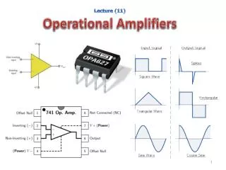
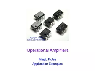
Dual In-line Package Small Out-line Package Microelectronic Circuits - Fifth Edition Sedra/Smith