Download
1 / 41
410 likes | 540 Views
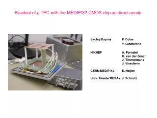
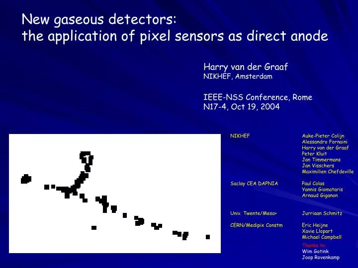
New gaseous detectors: the application of pixel sensors as direct anode. Harry van der Graaf NIKHEF, Amsterdam IEEE-NSS Conference, Rome N17-4, Oct 19, 2004. NIKHEF Auke-Pieter Colijn Alessandro Fornaini Harry van der Graaf Peter Kluit Jan Timmermans Jan Visschers

E N D
New gaseous detectors: the application of pixel sensors as direct anode Harry van der Graaf NIKHEF, Amsterdam IEEE-NSS Conference, Rome N17-4, Oct 19, 2004 NIKHEF Auke-Pieter Colijn Alessandro Fornaini Harry van der Graaf Peter Kluit Jan Timmermans Jan Visschers Maximilien Chefdeville Saclay CEA DAPNIA Paul Colas Yannis Giomataris Arnaud Giganon Univ. Twente/Mesa+ Jurriaan Schmitz CERN/Medipix Constm Eric Heijne Xavie Llopart Michael Campbell Thanks to: Wim Gotink Joop Rovenkamp
Original motivation: Si pixel readout for the Time Projection Chamber (TPC) at TESLA (now ILC)
Time Projection Chamber (TPC): 2D/3D Drift Chamber The Ultimate Wire (drift) Chamber track of charged particle E-field (and B-field) Wire plane Wire Plane + Readout Pads Pad plane
Wireless wire chambers: better granularity 1995 Giomataris & Charpak: MicroMegas
Wireless wire chambers: better granularity 1996: F. Sauli: Gas Electron Multiplier (GEM)
Problem With wires: measure charge distribution over cathode pads: c.o.g. is a good measure for track position; With GEMs or Micromegas: narrow charge distribution (only electron movement) avalanche GEM wire Micromegas Cathode pads Solutions: - cover pads with resisitive layer - ‘Chevron’ pads - many small pads: pixels
The MediPix2 pixel CMOS chip Cathode foil Drift Space Gem foils Support plate Medipix 2 We apply the ‘naked’ MediPix2 chip without X-ray convertor!
MediPix2 & Micromegas 55Fe Cathode (drift) plane Drift space: 15 mm Micromegas Baseplate MediPix2 pixel sensor Brass spacer block Printed circuit board Aluminum base plate Very strong E-field above (CMOS) MediPix!
55Fe, 1s No source, 1s 55Fe, 10s 14 mm Signals from a 55Fe source (220 e- per photon); 300 m x 500 m clouds as expected The Medipix CMOS chip faces an electric field of 350 V/50 μm = 7 kV/mm !! We always knew, but never saw: the conversion of 55Fe quanta in Ar gas
Single electron efficiency • no attachment • homogeneous field in • avalanche gap • low gas gain • • No Curran or Polya • distributions but simply: Prob(n) = 1/G . e-n/G Eff = e-Thr/G Thr: threshold setting (#e-) G: Gas amplification
New trial: NIKHEF, March 30 – April 2, 2004 Essential: try to see single electrons from cosmic muons (MIPs) Pixel preamp threshold: 3000 e- Required gain: 5000 – 10.000 New Medipix New Micromegas Gas: He/Isobutane 80/20 Ar/Isobutane 80/20 He/CF4 80/20 …… It Works!
He/Isobutane 80/20 Modified MediPix Sensitive area: 14 x 14 x 15 mm3 Drift direction: Vertical max = 15 mm
He/Isobutane 80/20 Modified MediPix
He/Isobutane 80/20 Modified MediPix
He/Isobutane 80/20 Non Modified MediPix Americium Source
He/Isobutane 80/20 Modified MediPix
He/Isobutane 80/20 Modified MediPix δ-ray!
After 24 h cosmic ray data and 3 broken chips: • We can reach very high gas gains with He-based gases (> 100k!) • The MedPix2 chip can withstand strong E-fields (10 kV/mm!) • Discharges ruin the chip immediately (broke 4 in 4 days!) • Measured efficiency: > 0.9; consistent with high gain • Seen MIPs, clusters, δ-rays, electrons, α ‘s…… • - In winter 2004: beam tests (dE/dX: e-, pions, muons,……), • X-rays (ESRF, Grenoble); • - Development of TimePix 1: TDC per pixel instead of counter
Integrate GEM/Micromegas and pixel sensor: InGrid ‘GEM’ ‘Micromegas’ Monolitic detector by ‘wafer post processing’
‘Try first Micromegas: simpel’ InGrid By ‘wafer post processing’ at MESA+, Univ. of Twente
HV breakdowns 1) High-resistive layer 3) ‘massive’ pads 2) High-resistive layer 4) Protection Network
Other application: GOSSIP: tracker for intense radiation environment: Vertex detector forSLHC
MIP Cathode foil CMOS chip ‘slimmed’ to 30 μm Drift gap: 1 mm Max drift time: 15 ns MIP Micromegas CMOS pixel array An thin TPC as vertex detector GOSSIP: Gas On Slimmed SIlicon Pixels
Essentials of GOSSIP: • Generate charge signal in gas instead of Si (e-/ions versus e-/holes) • Amplify # electrons in gas (electron avalanche versus FET preamps) • Then: • No radiation damage in depletion layer or pixel preamp FETs • No power dissipation of preamps • No detector bias current • Ultralight detection layer (Si foil+ 1 mm Ar gas) • 1 mm gas layer + 20 μm gain gap + CMOS (almost digital!) chip • After all: it is a TPC with 1 mm drift length (parallax error!) Max. drift length: 1 mm Max. drift time: 16 ns Resolution: 0.1 mm 1.6 ns
Ageing Power dissipation Material budget Rate effects Radiation hardness Efficiency Position resolution
Ageing Remember the MSGCs…… • Little ageing: • the ratio (anode surface)/(gas volume) is very high w.r.t. wire chambers • little gas gain: 5 k for GOSSIP, 20 – 200 k for wire chambers • homogeneous drift field + homogeneous multiplication field • versus 1/R field of wire. Absence of high E-field close to a wire: • no high electron energy; little production of chemical radicals • Confirmed by measurements(Alfonsi, Colas) • But: critical issue: ageing studies can not be much accelerated!
Power dissipation • For GOSSIP CMOS Pixel chip: • Per pixel: • - input stage (1.8 μA/pixel) • (timing) logic • Futher: data transfer logic • guess: 0.1 W/cm2 • Gas Cooling feasible!
Detector Material budget ‘Slimmed’ Si CMOS chip: 30 μm Si Pixel resistive layer 1 μm SU8 eq. Anode pads 1 μm Al Grid 1 μm Al Grid resistive layer 5 μm SU8 eq. Cathode 1 μm Al
Rate effects 0 Q 20 ns SLHC @ 2 cm from beam pipe: 10 tracks cm-2 25 ns-1 400 MHz cm-2! • ~10 e- per track (average) • gas gain 5 k • most ions are discharged at grid • after traveling time of 20 ns • a few percent enter the drift space: time • Some ions crossing drift space: takes 20 – 200 μs! • ion space charge has NO effect on gas gain • ion charge may influence drift field, but this does little harm • ion charge may influence drift direction: change in lorentz angle ~0.1 rad • B-field should help
Efficiency • Determined by gas layer thickness and gas mixture: • Number of clusters per mm: 3 (Ar) – 10 (Isobutane) • Number of electrons per cluster: 3 (Ar) - 15 (Isobutane) • Probability to have min. 1 cluster in 1 mm Ar: 0.95 • With nice gas: eff ~ 0.99 in 1 mm thick layer should be possible • But……. • Parallax error due to 1 mm thick layer, with 3rd coordinate 0.1 mm: • TPC/ max drift time 16 ns; σ = 0.1 mm; σ = 1.6 ns: feasible! • Lorentz angle • We want fast drifting ions (rate effect) • little UV photon induced avalanches: good quenching gas
Position resolution 0 Q 20 ns • Transversal coordinates limited by: • Diffusion: single electron diffusion 0 – 40/70 µm • weighed fit: ava 20/30 µm • 10 e- per track: σ = 8/10 µm • pixel dimensions: 20 x 20 – 50 x 50 μm2 • Note: we MUST have sq. pixels: no strips (pad capacity/noise) • Good resolution in non-bending plane! • Pixel number has NO cost consequence (m2 Si counts) • Pixel number has some effect on CMOS power dissipation • δ-rays: can be recognised & eliminated • 3rd (drift) coordinate • limited by: • Pulse height fluctuation • gas gain (5 k), pad capacity, # e- per cluster • With Time Over Threshold: σ = 1 ns ~~ 0.1 mm
Radiation hardness • Gas is refreshed: no damage • CMOS 130 nm technology: TID • NIEL • SEU: design/test • need only modest pixel input stage
Gas instead of Si • Pro: • no radiation damage in sensor • modest pixel input circuitry • no bias current, no dark current (in absence of HV breakdowns..!) • requires (almost) only digital CMOS readout chip • low detector material budget • low power dissipation • (12”) CMOS wafer Wafer Post Processing • no bump bonding • ‘simple’ assembly • operates at room temperature • less sensitive for X-ray background • 3D track info per layer • Con: • Gas chamber ageing: not known at this stage • Needs gas flow (but can be used for cooling….)
Plans • InGrid 1 available for tests in November: • rate effects • ageing (start of test: test takes years) • Proof-of-principle of signal generator: Xmas 2004! • InGrid 2: HV breakdowns, beamtests with MediPix (TimePix1 in 2005) • Gossipo: Multi Project Wafer test chip Dummy wafer
New gaseous detectors: the application of pixel sensors as direct anode Harry van der Graaf NIKHEF, Amsterdam IEEE-NSS Conference, Rome N17-4, Oct 19, 2004 NIKHEF Auke-Pieter Colijn Alessandro Fornaini Harry van der Graaf Peter Kluit Jan Timmermans Jan Visschers Maximilien Chefdeville Saclay CEA DAPNIA Paul Colas Yannis Giomataris Arnaud Giganon Univ. Twente/Mesa+ Jurriaan Schmitz CERN/Medipix Constm Eric Heijne Xavie Llopart Michael Campbell Thanks to: Wim Gotink Joop Rovenkamp