Download
1 / 2
20 likes | 154 Views
Photovoltaic effect in MoS 2 Schottky Diodes Paola Barbara, Georgetown University, DMR 1008242.

E N D
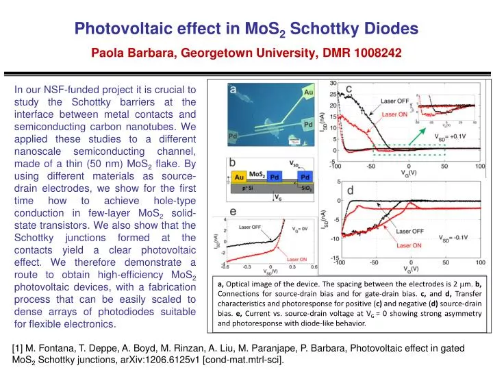
Photovoltaic effect in MoS2 Schottky DiodesPaola Barbara, Georgetown University, DMR 1008242 In our NSF-funded project it is crucial to study the Schottky barriers at the interface between metal contacts and semiconducting carbon nanotubes. We applied these studies to a different nanoscale semiconducting channel, made of a thin (50 nm) MoS2 flake. By using different materials as source-drain electrodes, we show for the first time how to achieve hole-type conduction in few-layer MoS2 solid-state transistors. We also show that the Schottky junctions formed at the contacts yield a clear photovoltaic effect. We therefore demonstrate a route to obtain high-efficiency MoS2 photovoltaic devices, with a fabrication process that can be easily scaled to dense arrays of photodiodes suitable for flexible electronics. Si a, Optical image of the device. The spacing between the electrodes is 2 mm. b, Connections for source-drain bias and for gate-drain bias. c, and d, Transfer characteristics and photoresponse for positive (c) and negative (d) source-drain bias. e, Current vs. source-drain voltage at VG = 0 showing strong asymmetry and photoresponse with diode-like behavior. [1] M. Fontana, T. Deppe, A. Boyd, M. Rinzan, A. Liu, M. Paranjape, P. Barbara, Photovoltaic effect in gated MoS2 Schottky junctions, arXiv:1206.6125v1 [cond-mat.mtrl-sci].
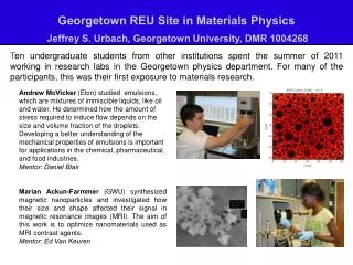
Photovoltaic effect in MoS2 Schottky DiodesPaola Barbara, Georgetown University, DMR 1008242 Kelvin Probe system Installation of new equipment: A custom designed Kelvin Probe system was installed and tested to measure work function of materials under ambient condition. Visit to Georgetown University (GU), Washington, USA: A Russian graduate student working with our Russian collaborators from the RRC-Kurchatov (Moscow) visited Georgetown University for one month (May 15 - June 15, 2012), to fabricate samples and learn about the Kelvin Probe system. GU undergraduate student: T. Deppe worked with GU graduate student A. Boyd and a visiting researcher from Brazil, M. Fontana, to fabricate MoS2 Schottky diodes. Russian graduate student, Igor Gayduchenko, working with GU graduate students. GU undergraduate student, Tristan Deppe, imaging a MoS2 flake with the AFM