Download
1 / 1
10 likes | 136 Views
Goal: Understand epitaxial growth of metals on metals Contributing factors include: lattice matching, surface energies, formation energies, strain energy Related work: "small" atoms (Ni, Fe, Pd, Co) form alloys at the Al surface (300 K); "large" atoms ( Ti ) form overlayer

E N D
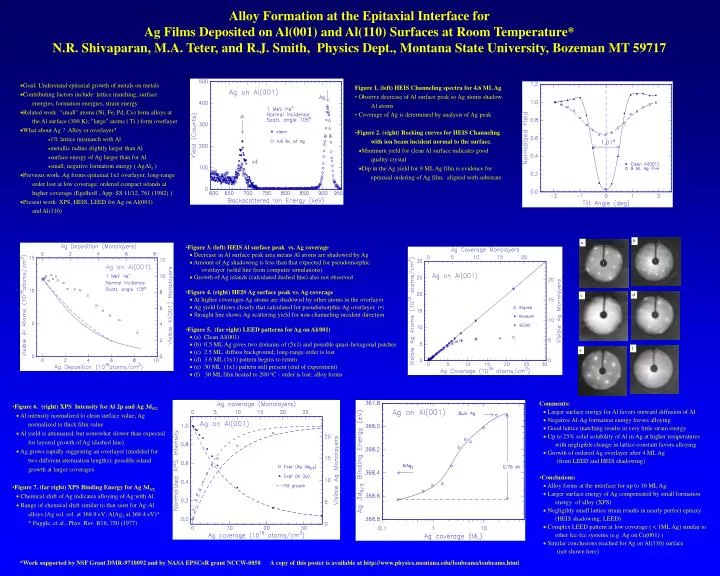
Goal: Understand epitaxial growth of metals on metals • Contributing factors include: lattice matching, surface energies, formation energies, strain energy • Related work: "small" atoms (Ni, Fe, Pd, Co) form alloys at the Al surface (300 K); "large" atoms ( Ti ) form overlayer • What about Ag ? Alloy or overlayer? • 1% lattice mismatch with Al • metallic radius slightly larger than Al • surface energy of Ag larger than for Al • small, negative formation energy ( AgAl2 ) • Previous work: Ag forms epitaxial 1x1 overlayer; long-range order lost at low coverage; ordered compact islands at higher coverage (Egelhoff , App. SS 11/12, 761 (1982) ) • Present work: XPS, HEIS, LEED for Ag on Al(001) and Al(110) • Figure 1. (left) HEIS Channeling spectra for 4.6 ML Ag • Observe decrease of Al surface peak so Ag atoms shadow Al atoms • Coverage of Ag is determined by analysis of Ag peak • Figure 2. (right) Rocking curves for HEIS Channeling with ion beam incident normal to the surface. • Minimum yield for clean Al surface indicates good quality crystal • Dip in the Ag yield for 9 ML Ag film is evidence for epitaxial ordering of Ag film, aligned with substrate Alloy Formation at the Epitaxial Interface for Ag Films Deposited on Al(001) and Al(110) Surfaces at Room Temperature*N.R. Shivaparan, M.A. Teter, and R.J. Smith, Physics Dept., Montana State University, Bozeman MT 59717 • Figure 3. (left) HEIS Al surface peak vs. Ag coverage • Decrease in Al surface peak area means Al atoms are shadowed by Ag • Amount of Ag shadowing is less than that expected for pseudomorphic overlayer (solid line from computer simulations) • Growth of Ag islands (calculated dashed line) also not observed • Figure 4. (right) HEIS Ag surface peak vs. Ag coverage • At higher coverages Ag atoms are shadowed by other atoms in the overlayer • Ag yield follows closely that calculated for pseudomorphic Ag overlayer () • Straight line shows Ag scattering yield for non-channeling incident direction • Figure 5. (far right) LEED patterns for Ag on Al(001) • (a) Clean Al(001) • (b) 0.5 ML Ag gives two domains of (5x1) and possible quasi-hexagonal patches • (c) 2.5 ML diffuse background; long-range order is lost • (d) 3.6 ML (1x1) pattern begins to return • (e) 30 ML (1x1) pattern still present (end of experiment) • (f) 30 ML film heated to 200 oC - order is lost; alloy forms • Comments: • Larger surface energy for Al favors outward diffusion of Al • Negative Al-Ag formation energy favors alloying • Good lattice matching results in very little strain energy • Up to 25% solid solubility of Al in Ag at higher temperatures with negligible change in lattice constant favors alloying • Growth of ordered Ag overlayer after 4 ML Ag (from LEED and HEIS shadowing) • Conclusions: • Alloy forms at the interface for up to 10 ML Ag • Larger surface energy of Ag compensated by small formation energy of alloy (XPS) • Negligibly small lattice strain results in nearly perfect epitaxy (HEIS shadowing; LEED) • Complex LEED pattern at low coverage ( < 1ML Ag) similar to other fcc-fcc systems (e.g. Ag on Cu(001) ) • Similar conclusions reached for Ag on Al(110) surface (not shown here) • Figure 6. (right) XPS Intensity for Al 2p and Ag 3d5/2 • Al intensity normalized to clean surface value; Ag normalized to thick film value • Al yield is attenuated, but somewhat slower than expected for layered growth of Ag (dashed line) • Ag grows rapidly suggesting an overlayer (modeled for two different attenuation lengths); possible island growth at larger coverages • Figure 7. (far right) XPS Binding Energy for Ag 3d5/2 • Chemical shift of Ag indicates alloying of Ag with Al • Range of chemical shift similar to that seen for Ag-Al alloys (Ag sol. sol. at 368.9 eV; AlAg2 at 368.4 eV)* * Fuggle, et al., Phys. Rev. B16, 750 (1977) *Work supported by NSF Grant DMR-9710092 and by NASA EPSCoR grant NCCW-0058A copy of this poster is available at http://www.physics.montana.edu/Ionbeams/ionbeams.html