Download
1 / 140
1.53k likes | 1.86k Views
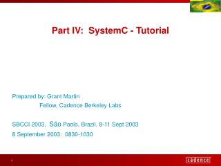
CADENCE Tools Lecture bases on CADENCE Design Tools Tutorial http://vlsi.wpi.edu/cds. Analog design flow. 7h Adder. CADENCE Tools for IC Design. Cadence is a set of different design tools used at different stages of the design process. Which tools we exactly need ?.

E N D
CADENCE Tools Lecture bases on CADENCE Design Tools Tutorial http://vlsi.wpi.edu/cds VLSICirciuit Design
Analog design flow 7hAdder VLSICirciuit Design
CADENCE Tools for IC Design Cadence is a set of different design tools used at different stages of the design process. Which tools we exactly need ? Composer -> Schematic editor Virtuoso -> Layout editor Analog Artist–> preparing simulation (SpectreS in this tutorial) DIVA –> Design Rule Check (DRC) , Layout Versus Schematic Check (LVS) , Extraction VLSICirciuit Design
First steps with Cadence • To start Cadence software enter: icfb & • The cadence window after start up: • To see your cadence libraries open Library Manager from „Tools menu” VLSICirciuit Design
First steps with Cadence • Cadence libraries: • Technological Libraries (usually names written with upper cases) • User Libraries • Libraries contain cells – basic elements of your design • Every cell may have different views – different views created at different stages of the design and edited with different tools VLSICirciuit Design
Creating new libraries and cells • In File on the menu of Library Manager choose New -> Library or Cellview. • Examplarty „Creat New File window” Library NameChoose your working directory and library name Cell NameEnter the cell name View NameEnter view name depending onthe level of the design hierarchy. Eg. schematic or layout VLSICirciuit Design
Design ExampleCMOS -Inverter VLSICirciuit Design
Creating Schematics • The traditional method for capturing (i.e. describing) your transistor-level or gate-level design is via the schematic editor. • Schematic editors provide simple, intuitive means to draw, to place and to connect individual components that make up your design. • The resulting schematic drawing must describe the main electrical properties of all components and their interconnections. VLSICirciuit Design
Open a new schematic window • View Name Indicates the level of the design hierarchy.The correct view name choice is "schematic" for our example. • Click OK to finish VLSICirciuit Design
Add components • The first thing to do is to add and place components which will be used in the schematic. • We need the componets as folow: • PMOS : p-type MOSFET • NMOS : n-type MOSFET • VDD : vdd! global net marker • GND : gnd! global net marker VLSICirciuit Design
Add components • Add Component Window Enter the Library Name, Cell Name and the View Name of the component • Component Browser enables the designer to browse easily through the available libraries and select the desired components. VLSICirciuit Design
Add components • Pick up the MOS transistors from the Component Browser window. • Open the "N_Transistors" folder by clicking once on it. • Pick up the NMOS transistor by clicking once on "nmos", which is a model for a three terminal n-type MOSFET. VLSICirciuit Design
Add components • Click on a location in the schematic window, where you want to put the transistor. • Use the same procedure to select and to place the PMOS transistor. Picking up the supply voltage components involves the same steps as in adding transistors to the schematic. VLSICirciuit Design
Conecting components To connect the components in a schematic, we use wires by choosing Add and then Wire (narrow) on the menu banner. VLSICirciuit Design
Conecting components Connecting any two nets in the schematic is done by first clicking at one of the nets and then at the other one. Press ESC key to leave the wiring mode. VLSICirciuit Design
Edit properties of components <=1. Select component by clicking on it 2. Choose Properties => and then Object from the Edit menu. VLSICirciuit Design
Edit properties of components • Edit the properties => • by clicking on the corresponding field. You may change the values for Width or Length depending on your design specifications. VLSICirciuit Design
Edit properties of components 4.Click OK after => editing the properties in the Edit Object Properties Window. The most important parameters always appear in the schematic window. VLSICirciuit Design
Placing the pins You must place I/O pins in your schematic to identify the inputs and the outputs. • Click Add on the => menu and then select Pin on the pull-down menu. VLSICirciuit Design
Placing the pins 2.Enter the name of your pins in the Pin Names field. Choose the direction. Place pins by clicking on a lcoation in the schematic window. VLSICirciuit Design
Placing the pins Connect the => pins to the corresponding nodes using wires. The wiring procedure is the same as described in the previous steps. VLSICirciuit Design
Check and Save Click Design on the menu banner => and then select Check and Save. <= Check the message field every time you save a design. VLSICirciuit Design
Creating cellview If a certain circuit design consists of smaller hierarchical components (or modules), it is usually very beneficial to identify such modules early in the design process and to assign each such module a corresponding symbol (or icon) to represent that circuit module. VLSICirciuit Design
Creating cellview From the Design menu, select Create Cellviewand then From => Cellview <= Check the view names You have to ensure that the target view name is symbol. VLSICirciuit Design
Locating the pins After clicking OK in the Cellview From Cellview, window the following window pops up : • Edit your pin attributes and locations. In the default case, you will have your • input(s) on the left of the symbol • output(s) on the right of the symbol. Change pin locations by putting the pin name in the corresponding pin location field VLSICirciuit Design
Editing the shape of the symbol icon In the new window, the automatically generated symbol is shown. VLSICirciuit Design
Editing the shape of the symbol icon • You can do the following operations on your symbol • Deleting/replacing some existing parts • Adding new geometric shapes • Changing the locations for pins and instance name • Adding new labels VLSICirciuit Design
Check and Save – Once Again • Save – doesn’t check anything. • Checking a symbol means comparing the symbol view with the corresponding schematic view, by matching all of the pin names. To check and save the symbol, choose Check and Save from the Design menu VLSICirciuit Design
Simulation • The electrical performance and the functionality of the circuit must be verified using a Simulation tool. • Based on simulation results, the designer usually modifies some of the device properties. VLSICirciuit Design
Simulation -New Schematic Design • 1.Open a new schematic. • Follow the same procedure described in „Open a new schematic" to create a new schematic where you will put your simulation schematic for the inverter. • Give a name to your new schematic which makes it clear that the new schematic is to simulate the inverter. • Note : You should first create the symbol of the circuit schematic which you want to simulate VLSICirciuit Design
Simulation - Select and place components • The first step is to add and to place the components which will be used to simulate the inverter. • The components we need for the simulation of the inverter are the following : • Inverter - Symbol created for the inverter • VDD - Power supply voltage • GND - Ground line • vdc - DC voltage source • vpulse - Pulse waveform generator • C - Capacitor VLSICirciuit Design
Simulation - Select and place components How to pick up a symbol from library, and to place it in the schematic ? <= To pick up the inverter symbol, change the library of the Component Browser to library, "tutorial". VLSICirciuit Design
Simulation - Select and place components • After the library "tutorial" is selected, there will be a new list of • components which are included in this library • every symbol that you created within this library will show up here. By clicking on "inverter" in the component list in the Component Browser, you can pick up the symbol you created for the inverter VLSICirciuit Design
Simulation - Select and place components You can go to the schematic window and place the symbol of the inverter to a point by clicking on it VLSICirciuit Design
Simulation - Select and place components • Pick up and place the rest of the components required for the simulation. • Place the supply nets, "vdd" and "gnd". • Place the voltage sources, "vdc" and "vpulse". • Place the capacitance which will be the output load, "cap". Match placed componets as was showed on the picture. Use the same method as previously. VLSICirciuit Design
Simulation - Define the voltage source VDC A DC-voltage source called "vdd" is required as the power supply voltage in all digital circuits. The value of this voltage usually depends on the technology used. Edit the DC voltage field in=> the Edit Object Properties window and type the VDD value which is 3.3V VLSICirciuit Design
Simulation - Define the voltage source Vpulse • The pulse generator is a voltage source which can produce pulses of any duration, period and voltage levels. • This source will be used to generate the input data How to use parameters to define the input pulse waveform ?=> VLSICirciuit Design
Simulation - Define the voltage source Vpulse The values for the=> pulse generator parameters which are used to define the input waveform. Change them using the method as previously. VLSICirciuit Design
Simulation - Define the voltage source - results VLSICirciuit Design
Simulation - Determine the output load Edit the properties of the capacitor which is the output load of the inverter. Change capacitance => from the default value (1 pF) to 25 fF VLSICirciuit Design
Simulation – Adding labels • labeling a node = adding names to the wires. • it allow to observe important nodes (or wires) during simulations. • adding pins (during drawing the schematic) labeling a node How can I do it ? First, select Wire Name in the Add command list. => VLSICirciuit Design
Simulation – Adding labels • type all the label names one after the other in the Names field • there isn't any information related to the direction of the nodes - only the pins are defined with a direction. We will label the two wires as "in" and "out". VLSICirciuit Design
Simulation – Adding labels • After all the labels are typed, move the mouse cursor on the schematic • You will see the first label floating with the mouse cursor. Click on the corresponding net to name the net with this label. • As soon as you put the first label, the second label will appear on the mouse cursor. • This procedure is repeated until you are finished putting all label names you entered in the Add Label window. VLSICirciuit Design
Simulation – Adding labels results Note:Save your design by using Check and Save in the Design command list. Be sure that the CIW doesn't report any errors or any warnings. VLSICirciuit Design
Simulation - Open the simulator window <= Open the Analog Artist window. VLSICirciuit Design
Simulation - Edit the Simulation Parameters • there are many available analysis options you can choose. • each of these options provides a specific sub-region within the Choosing Analysis window. We want to obtain the delay information for the inverter, we choose the transient simulation type, so that the output can be traced in time domain. VLSICirciuit Design
Simulation - Edit the Simulation Parameters In the Transient Analysis region, type a value in the Stop Time field to determine how long the simulation will take place. VLSICirciuit Design
Simulation - Run the Simulation • click on Outputs in the Analog Artist Simulation menu banner • select To Be Plotted and then Select on Schematic. • when the schematic window becomes automatically active, select the nodes to be observed VLSICirciuit Design
Simulation - Run the Simulation <= Start the simulation by clicking Simulation and then selecting Run. VLSICirciuit Design
Simulation - Run the Simulation The waveform window appears after the simulation is completed. VLSICirciuit Design