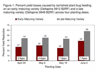
Download
1 / 16
180 likes | 637 Views
Dose Map and Placement Co-Optimization for Timing Yield Enhancement and Leakage Power Reduction. Kwangok Jeong, Andrew B. Kahng, Chul-Hong Park, Hailong Yao University of California, San Diego. Background. Critical dimension (CD) variation

E N D
Dose Map and Placement Co-Optimization for Timing Yield Enhancement and Leakage Power Reduction Kwangok Jeong, Andrew B. Kahng,Chul-Hong Park, Hailong Yao University of California, San Diego
Background Critical dimension (CD) variation Dominant factor in the variation of delay and leakagecurrent of transistor gates Equipment improvement Opportunity to leverage design information for cost and turnaround time improvements ASML’s DoseMapper technology Extensively used to improve global CD uniformity We explore a method that DoseMapper can be usedto improve design parametric yield
Motivation Motivation Use DoseMapper to improve device performance andparametric yield Idea Increase dose decrease gate CD of timing critical device more speed Decrease dose increase gate CD of non-timing critical device less leakage power Methods Dose map optimization method: given placement,optimize the dose map Placement optimization method: given dose map,optimize the placement
DoseMapper Fundamentals DoseMapper Devised to adjust exposure dose to improveCD uniformity Compensate for CD error induced byACLV and AWLV Unicom (slit direction) Change intensity profile across slit Actuator is a variable-profile gray filter inserted in the light path Maximum correction range: +/- 5% by changingthe shape of gray filter Dosicom (scan direction) Change intensity profile along scan direction Dose profile can contain higher-order corrections Maximum correction range: +/-5% by changing the dose energy of the laser Dose Sensitivity Linewidth has an approximately linear relationship with the exposure dose Dose sensitivity (DS): -2nm/% Scan Direction Slit Direction Adjust exposure dose Slit and Scan directions
Delay and Leakage vs. Gate Length Partition the exposure field into grids: Gate length changes linearly with dose tuning: Lg: gate length change di,j: change of dose in grid ri,j Linear relation between the change of gate delay and the change of exposure dose: A:experimentally decided parameter • Assume quadratic relation between the change of gate leakage and the change of exposure dose:
Method 1: Placement-Aware Dose Map Objective Given placement P with timing analysis results, determine the dosemap to improve timing and total leakage power Basic method Assume that gate delay increases linearly, but leakage power decreases quadratically as gate length increases Partition the exposure field into a set of grids The formulation can be solved by a quadratic programming methods like CPLEX • Ap, p, p are calibrated from pre-characterized timing and leakage libs • Wire delay from timing analysis are added in between gates
Method 1: Placement-Aware Dose Map (2) Our Proposal: different CDs DoseMapper: same CDs • Device on setup-timing critical path larger dose faster-switching transistors • Device on hold-timing critical path smaller dose less leaky transistors • Improve timing yield withoutleakage penalty • Improve global CD uniformity achieve the same gate CD in all devices • Does not address device yield improvement • No “design awareness’’
Method 2: Dose Map-Aware Placement Cell swapping-based placement Given an original placement result and a timing and leakage-aware dose map, determine cell pairs and swap those pairs for timing yield improvement Basic idea Swap critical cells to high-dose regions and non-critical cells to low-dose regions, to enhance the circuit performance Fast filter Bounding box of net Bound on distances between cell pairs HPWL-based wire length comparison Priority of cells during swapping Number of critical paths passing through the cell Slacks of critical paths Weight of a cell: Number of swaps Unnecessary to swap all the cells to eliminate a critical path Threshold on number of cells swapped for each path Cell a Cell b Cell c Cell d Cell e NAND Bounding box of NAND cell
Method 2: Dose Map-Aware Placement (2) D1 Dose (D1) path P1 path P1 path P2 path P2 D2 Dose (D2) After Cell-Swapping Before Cell-Swapping Dose: D1<D2, Timing Criticality: P1>P2 • Objective: Given an original placement result and a timing and leakage-aware dose map, determine cell pairs and swap those pairs for timing yield improvement • Method: Swap critical cells to high-dose regions and non-critical cells to low-dose regions, to enhance the circuit performance • Fast filter: HPWL-based wire length comparison using bounding box • Priority: (1) Number of critical paths passing through the cell (2)Slacks of critical paths
Timing and Leakage Optimization Flow Dose Map opt Input Coeff calibration Timing analysis Dose map opt Optimal dose map Placement opt Update design Timing analysis Critical path identification Dose-aware place Legalization ECO routing Design Timing Analysis Original Dose map Dose map Opt. Delay Cell Library Dose Map Optimal Dose Map Timing Analysis Updated Design Placement Critical Path Placement Opt. Optimized Design
Dose Map Optimization Flow Input Original dose map Characterized cell libraries Slew, cap, cell and wire delay Delay and leakage coeffs calibration from cell libraries Chip partition Dose variable creation Build timing graph Generate quadratic program QP solver Output: optimal dose map Input Netlist extraction Coefficients calibration Delay variable generator Quadratic program generator Chip partition Quadratic program solver Dose variable creation Output
Dose Map Optimization Results • AES • Block Size: 0.25 mm2 • #Cell Instances: 21944 • #Nets: 22581 • JPEG • Block Size: 1.09 mm2 • #Cell Instances: 98555 • #Nets: 105955 • Rectangular grids: 20 50 • Dose correction range: 5% • : a scaled value to balance between delay and leakage power • Over 8% timing improvement
Dose Map and Placement Co-Optimization • Rectangular grids: 20 50 • Dose correction range: 5% • Cell-swapping based dosePl further improves timing • 9.6% for AES • 8.9% for JPEG
Slack Profile Worst slack of the original design is optimized a lot by dose map optimization process Much smaller optimization space left for the following placement process The difference between the worst slacks of dose-optimized design and the biased design (“best” design) is quite small (0.05ns) In the dose map-optimized design,the number of critical paths, whose slack values are near the worst slack value, is large. The placement process has to swap many cells to further improve timing AES: slack profiles of original design, the design after dose map optimization and the design when all the gates in the top 10000 critical paths are enforced using maximum possible dose
Summary The exposure dose in the exposure field can change the gate/transistor lengths of the cells in the circuit Useful for optimization of gate delay and gate leakage power We have proposed to improve the timing yield of the circuit as well as reduce total leakage power, using design-aware dose map and dose map-aware placement optimization We focus mainly on the placement-aware dose map optimization Experimental results are promising More than 8% improvement in minimum cycle time of the circuit at no cost of leakage power increase Ongoing work Testing on more test cases, especially on larger industrial 65nm designs Clock skew optimization