Download
1 / 2
20 likes | 23 Views
Everything is twirled under the semiconductor robot handling. The results can likely be obtained via anyone with just merely looking over to it. We can also consider it as an initiation of the semiconductor revolution.

E N D
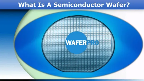
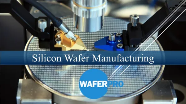
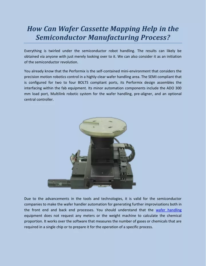
How Can Wafer Cassette Mapping Help in the Semiconductor Manufacturing Process? Everything is twirled under the semiconductor robot handling. The results can likely be obtained via anyone with just merely looking over to it. We can also consider it as an initiation of the semiconductor revolution. You already know that the Performix is the self-contained mini-environment that considers the precision motion robotics control in a highly-clear wafer handling area. The SEMI compliant that is configured for two to four BOLTS compliant ports, its Performix design assembles the interfacing within the fab equipment. Its minor automation components include the ADO 300 mm load port, Multilink robotic system for the wafer handling, pre-aligner, and an optional central controller. Due to the advancements in the tools and technologies, it is valid for the semiconductor companies to make the wafer handler automation for generating further improvisations both in the front end and back end processes. You should understand that the wafer handling equipment does not request any meters or the weight machine to calculate the chemical proportion. It works over the software that measures the number of gases or chemicals that are required in a single chip or to prepare it for the operation of a specific process.
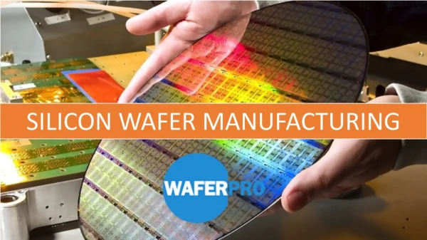
The foremost technical challenge is to minimize the number of particles generated by the robots and provide damage-free wafer handling with other substrates. There are two unique categories of substrate wafer handling robots in general: atmospheric robots and vacuum robots. The atmospheric robots would perform at the elemental atmospheric pressure. In contrast, the vacuum robots get performed at extremely clean enclosures, either they are present in the vacuum or in certain gas environments. The wafer cassettes have a major use for storage and wafers transport purposes in the semiconductor manufacturing working process. These are mainly known as the wafer carriers for most people. These are designed in a manner to carry several kinds of wafers of particular sizes. Have a look at the following dimensions of the wafer cassettes: • line and the wafer pocket. Pocket Spacing: It is generally calculated as the whole distance between every center D1 dimension: The D1 dimension also depicts the whole distance from a single end of • the cassette to the centerline wafer pockets. Pocket Flat: It is considered the label that gives back to the wafer pockets width at a • very nano west distance. The significant role of the wafer handling of the front end and back end is read under the wafer robot stage with the Kensington Laboratories' repairing. The Kensington Laboratories has a significant focus on the main edge semiconductor innovation that bestows the major and extensive experiences to the applications arriving in the future. Infact the requirements drive adjustments in the semiconductor assembly and the semiconductor front end manufacturing techniques. You must know the outdated items, long lead times, segment lack, and the semiconductor parts' dread getting in sequel into the flexible chain. The constant fake fear is all dependent upon the cloned gadgets, which is considered in opposition to taking it from the very first item and the emerging warning of the digital assaults. The Semiconductor Wafer Handling Robots have the potential to offer a perfect view of the needs of the semiconductor quartz and wafer handling. At Kensington Laboratories, we provide a full line of industry-leading semiconductor wafer handling robots. Consult our team today for more information on this. Get the best and reliable assistance from Kensington Laboratories today!