Download
1 / 21
220 likes | 534 Views
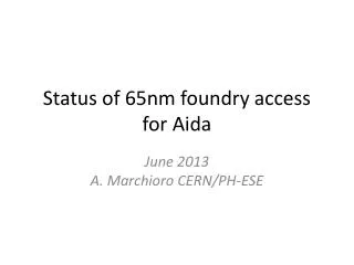
Status of CMOS 65nm technology access, distribution and IP blocks development. Microelectronics User Group TWEPP 2013. Sandro Bonacini CERN, PH-ESE dept. CH1211, Geneve 23 Switzerland. O utline. Motivation for use of 65 nm CMOS technology Radiation performance

E N D
Status of CMOS 65nm technology access,distribution and IP blocks development Microelectronics User GroupTWEPP 2013 Sandro Bonacini CERN, PH-ESE dept. CH1211, Geneve 23 Switzerland
Outline • Motivation for use of 65 nm CMOS technology • Radiation performance • Technology options for 65 nm • Devices • Metal stack • Libraries • Design automation solutions for 65 nm • Mixed Signal Design kit • Mixed Signal Workflows • IP Blocks • Technology distribution scheme for 65 nm • Maintenance • Training • Support • Foundry access • Access to new 130 nm technology Sandro Bonacini - PH/ESE - sandro.bonacini@cern.ch
Motivation • Future vertex detectors for high energy physics experiments can benefit from modern deep submicron technologies • Scaling is necessary to improve the performances of pixel detectors • Smaller pixel sizes (pitch) • More “intelligence” in each pixel • Faster serializers/deserializers • In general, the expected advantages in porting a front-end circuit to a more advanced technology include • A much more compact, faster digital part (reduction in area of ~60% compared to 130nm technology) • Better matching than in 130nm • Results of radiation hardness studies are encouraging • See https://iopscience.iop.org/1748-0221/7/01/P01015/ , “Characterization of a commercial 65 nm CMOS technology for SLHC applications” • And from CPPM (M.Menouni): http://indico.cern.ch/materialDisplay.py?contribId=2&materialId=slides&confId=271338 Sandro Bonacini - PH/ESE - sandro.bonacini@cern.ch
Radiation performance • Core transistors • Very small threshold voltage shifts (<60mV @200Mrad) and leakage current • No ELT necessary for digital core logic • PMOS loss of drive current above ~50 Mrad • WPMOS>1um helps limiting drive/speed loss • I/O devices still need Enclosed Layout Transistors (ELT) • PMOS loss of drive current (-transconductance & +threshold voltage) • …needs to be oversized! (or avoided) • SEU performance is better as sensitive areas are smaller • ~4x cross-section reduction with respect to 130nm • But beware in using more logic in chips • More evident MBUs • Observed up to 10-bit upsets in SRAM @1.2V, LET=20.4 MeVcm2/mg • MBU contribution in D-FF registers is ~0.5% due to 2-BU and 3-BU. Sandro Bonacini - PH/ESE - sandro.bonacini@cern.ch
On-going projects in 65 nm • Phase-2 upgrades • RD53: high-rate pixel detector for ATLAS and CMS • http://indico.cern.ch/contributionDisplay.py?contribId=27&confId=252473 • CMS tracker: Macro Pixel ASIC (MPA), tracking trigger • http://indico.cern.ch/contributionDisplay.py?contribId=34&sessionId=9&confId=153564 • http://pos.sissa.it/archive/conferences/137/037/Vertex%202011_037.pdf • Internal PH/ESE • Low-Power Gigabit Transceiver (LPGBT) • D.Felici et al. “A 20 mW, 4.8 Gbit/sec, SEU robust serializer in 65nm for read-out of data from LHC experiments” in this workshop: • http://indico.cern.ch/contributionDisplay.py?contribId=184&sessionId=6&confId=228972 • CLICpix • P.Valerio et al. “A prototype hybrid pixel detector ASIC for the CLIC experiment” in this workshop: • http://indico.cern.ch/contributionDisplay.py?contribId=76&sessionId=6&confId=228972 • Other talks in this conference: • FE-T65-1: ATLAS pixel detector front-end • M.Havranek et al., “Pixel front-end development in 65 nm CMOS technology” • https://indico.cern.ch/contributionDisplay.py?confId=228972&contribId=2 • AMchip: pattern recognition stage of the Fast TracKer (FTK) processor for ATLAS • M.M.Beretta et al. “Next generation Associative Memory devices for the FTK tracking processor of the ATLAS experiment” • https://indico.cern.ch/contributionDisplay.py?sessionId=6&contribId=50&confId=228972 Sandro Bonacini - PH/ESE - sandro.bonacini@cern.ch
Drawbacks of using 65 nm technology Higher cost of tape-out compared to older technologies Strong push for 1st working silicon Push for more IP re-usage? Must limit technology options usage Higher gate leakage current More stringent design rules: ELT transistors are not allowed, more difficult to achieve an optimal layout. OPC rules: avoid jogs, zigzag, shapes like “L”, “U” or ring, … Deep submicron technologies are not optimized for analog designs Smaller dynamic range due to the lower power supply reduces the possibilities to use some structures (such as cascoded stages). Multiple stages, with possible stability issues, are needed to achieve a high gain. This problem is moreover aggravated by the lower output resistance of the MOSFETs which lowers the gain of the single stages. Sandro Bonacini - PH/ESE - sandro.bonacini@cern.ch
Technology options & costs • Many tech. options but they all come at a cost • Options modulate strongly the manufacturing cost • Must be taken into account at early design stages • Thin metals are expensive because of their fine pitch • Metal levels • Thin metals • W+S = 100+100nm • thickness ~W • Top metals • Thick: W+S = 400+400nm, T~~2W • Ultra-thick: W+S = 2+2um, T~~1.5W • Last metal, redistribution layer (RDL) • used for pad (WB and bump), interconnection, laser fuses • Can be Al or Cu • thickness ~~ 3 um • Devices • Transistors • Standard-, high-and low-Vt • Low-vt devices have high leakage • ~4 nA/um • Standard-vt is high for typical analogapplications • Limited dynamic range • ...or low-voltage architectures needed • Low- and high-vt are expensive options! • zero-vt (native) • Triple well • Junction diodes: N+/PW, P+/NW, NW/Psub • MIM capacitors • Costly option, maybe possible to use instead Vertical Natural Capacitors (VNC, VPP, MOM, …) • High-Q inductors • Fabricated with Ultra-Thick Metal (UTM) Sandro Bonacini - PH/ESE - sandro.bonacini@cern.ch
Supported metal stacks and libraries passivation RDL RDL M6 M6 M5 M5 M5 mimcap M4 M4 M4 M3 M3 M3 M3 M2 M2 M2 M2 M1 M1 M1 M1 M1 M1 W W W W W poly poly STI Sandro Bonacini - PH/ESE - sandro.bonacini@cern.ch • CERN mixed signal (M/S) kit will be supported for: • 2 metal stacks • 6+1 metals (“CERN metal stack”) • 4-thin, 1-thick, 1-UTM , RDL • 9+1 metals (compatible with IMEC mini@sic) • 7-thin, 1-thick, 1-UTM , RDL • + 220 k$ for mask set (!) • 2 choices of std. cell libraries • 9-tracks, standard-Vt • 7-tracks, high-Vt
Motivation for a Mixed Signal flow Third party IP vendors Foundry PDKs 90 nm 45 nm 130 nm 65 nm Methodologies CAE Tools • New technologies require a stronger organization of design methodologies • 65 nm presents stricter design rules, more complex RC extraction, must be verified more carefully (more corners, Montecarlo), etc. • A complex design environment • Projects with large, fragmented, multinational design teams. • Powerful and flexible CAE Tools but complicated to use. • Third party digital cell IP libraries primarily prepared for the back-end design flow. • Designs of increased complexity (SOC). • A uniform set of tools and an uniform way of using them, for every designer is necessary • All design teams have to conform to a common design workflow • Benefits: • Design productivity improvements and reduced design cost • Successful silicon-accurate designs. • More manageable technical support services. Sandro Bonacini - PH/ESE - sandro.bonacini@cern.ch
PDK and Mixed Signal Design kit • Objectives • Development of a “Design Kit” for Mixed Signal environments. • With integrated standard cell libraries. • Establish well defined Analog & Mixed Signal design workflows. • Implemented on modern versions of CAE Tools. • Physical Layout views available. • Suitable for analog, digital and mixed design • Foundry database not made for full M/S interoperability • Technology library and PDK in OA (and CDB) • Digital libraries in CDB only • Must be ported to OA for full M/S flow • Integration work done by VCAD (Cadence) • Many modifications in the technology file • Validated by CERN • Work with VCAD started Apr. 2013 • Preliminary version delivered to CERN this month • Final version target date: 31st October 2013
M/S flow and features Analog Schematic entry Analog simulation Full-custom layout Parasitic extraction Analog simulation M/S simulation M/S simulation Abstract generation Signoff Digital HDL code Synthesis P&R Digital simulation Digital simulation Parasitic extraction • Develop and validate design flows to allow analogand digital design interoperability. Sandro Bonacini - PH/ESE - sandro.bonacini@cern.ch
M/S design kit contents N65OA • V1.7A_1_VCADstack6 • V1.7A_1_VCADstack9 • Calibre • PVS • Libraries … • tsmcN65 • PDK_doc • models • 7-tracks hVt • std cells • 9-tracksstd cell • IO Pads Sandro Bonacini - PH/ESE - sandro.bonacini@cern.ch
Supported versions of CAE Tools • Flow constructed to be fully compatible with the Europractice distribution tools • Calibre is recommended but optional (alternative is Assura PVS) Sandro Bonacini - PH/ESE - sandro.bonacini@cern.ch
Rad-hard libraries • Standard cell & IO pad libraries from foundry suffer from radiation effects • NMOS leakage • PMOS tend to turn off + loss in transconductance • Re-characterize standard cells libraries • PMOS drive loss results in speed loss with TID (above ~50Mrad) • Create standard cell library timing (liberty file) for radiation corner • Develop Radiation hardened I/O pad library • Rated for 1.2V or 1.0V • Only core devices, thin gate oxide • Subcontract the development work for rad-hard ESD circuitry • Access to layout views & modification allowed by foundry • Clause of no-redistribution except to signatories of NDA (list to be updated annually) • Discharge of any foundry liability for modified libraries • Modified library has to be given back to foundry • Library NOT to be used with other foundry !!! Sandro Bonacini - PH/ESE - sandro.bonacini@cern.ch
Rad-hard IP Blocks • Rad-hard SRAM compiler • Single-port / pseudo-dual-port • Minimum size: 128 words of 8 bit • Max size: 1k words of 256 bits • Specifications on minimum W of transistors to avoid leakage and drive loss • WPMOS>500nm, WNMOS>200nm • Design outsourced Jul. 2013 • Delivery expected Jan. 2014 • ADC, bandgap • Delivery expected 2014,Q2 • ADC: 32 channels, 12 bit, 1 MS/s, 1 V full scale, power <2mW Sandro Bonacini - PH/ESE - sandro.bonacini@cern.ch
M/S flow distribution Foundry • Distribution of package to institutes done by IMEC • Sign NDA with institutes • Distribute the M/S design kit and workflows • Provide maintenanceand updates in collaboration with VCAD IMEC Cadence VCAD design services CERN Physics institutes Sandro Bonacini - PH/ESE - sandro.bonacini@cern.ch
NDA IMEC to deliver NDA to institutes Sandro Bonacini - PH/ESE - sandro.bonacini@cern.ch
Training: M/S kit Workshops Example Mixed Signal ASIC: “8-bit DAC with I2C serial interface” • A series of Training Workshops for 65nm CMOS will be organized • To present the Mixed Signal Kit. • To present Analog, Digital and Mixed Signal design Workflows. • Scheduled for February 2014 • At IMEC or at CERN • Cadence (VCAD) design services team: • Will prepare the training lectures and the accompanying documentation • Will provide engineers to lecture in the courses. • 3 days training with lectures and hands-on design exercises • Workshop modules based on a realistic Mixed Signal Design • Training material (scripts, design examples and documentation) made available to participants. Sandro Bonacini - PH/ESE - sandro.bonacini@cern.ch
Foundry Access Services CERN Physics institutes IMEC Foundry • Foundry Access • MPW as scheduledfrom IMEC and foundry • Foundry run every 2 weeks • mini@sic metal stack • 7-thin, 1-thick, 1-UTM • Additional runs for HEP • Metal stack 4-thin, 1-thick, 1-UTM • Possibly every 4 months? • Engineering/production runs • Physics institutes to send the purchase order via CERN • GDS will be submitted directly to IMEC Sandro Bonacini - PH/ESE - sandro.bonacini@cern.ch
Access to alternate 130 nm process • Contract with foundry includes access to older technology nodes: 130 nm • The same scheme of M/S kit development and distribution will be applied to 130 nm • CERN would continue to work with IBM and the new foundry in parallel • Libraries and metal stack To Be Defined • 013 for MS or RF ?? • 8 metals (5 thin, 1 thick, 1 UTM, RDL) ?? • Radiation Hardness must be investigated Sandro Bonacini - PH/ESE - sandro.bonacini@cern.ch
Conclusions • Integrated OA PDK and digital library in 65 nm • For Mixed Signal System-On-Chip design • Standardized workflows • Roles of IMEC include: • Maintenance • Training • Support • Foundry access • Cadence VCAD can provide development and help when necessary • The same concept to be applied in 130 nm • Future plans • Outsource design of ESD structures and CMOS I/O standard pad library • Acquire rad-hard SRAM compiler • Further investigation on radiation performance • Re-characterize standard cell library for lower Vdd Sandro Bonacini - PH/ESE - sandro.bonacini@cern.ch