Download
1 / 8
80 likes | 140 Views
EUDET FP7 brainstorm. EUDET-JRA2 Jan Timmermans. My personal opinion…. I would be in favour of waiting till next call Because “grand” particle physics proposal seems to create a lot of extra overhead and may thus become ‘unmanageable’

E N D
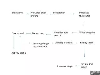
EUDET FP7 brainstorm EUDET-JRA2 Jan Timmermans
My personal opinion…. • I would be in favour of waiting till next call • Because “grand” particle physics proposal seems to create a lot of extra overhead and may thus become ‘unmanageable’ • On the other hand: EUVIF seems a good way to continue EUDET
After some discussions with Ties….Possible topics/workpackages: • As “integration facility”: Micro electronics facility (real synergy with other JRA’s) • Would a ~4T magnet (of reduced size) be possible? What size? Costs? • Global Detector Network • Under WP7 “Tracker prototype infrastructure”: could that include further development of Timepix? (and/or large pixel endplate?). Again synergy with e.g. SLHC upgrades, see proposal Michael Campbell @ Paris meeting
Test structures (TS) as an infrastructure item IEKP Karlsruhe, HEPHY Vienna • Common solution to quickly evaluate all necessary sensor parameters of new sensors during • R&D • Full production • Establishment of a full package • TS layout and masks • Description of measurement equipment • full software, including exchange and comparison protocols • This infrastructure item needs the involvement of industry to build first TS prototypes • Useful for ILC and SLHC and …
Monitoring the R&D and later the Fabrication Process of Silicon Sensors using dedicated Test Structures Utilize space left on wafer for test structures. Determine one process parameter per structure. Allows measurement of parameters not accessible on the main detector Allows destructive measurements not possible on the main sensor. Used for CMS and was a great success diode GCD baby MOS 2 TS-CAP CAP-TS-AC CAP-TS-AC MOS 1 sheet
Test structures Measurement Setup Probe-card with 40 needles contacts all pads of test structures in parallel Crosspoint switching box connects Instruments to needles Labview and GPIB used to control instruments and switching system Parameters being tested: depletion voltage and bulk resistivity Bulk dark current and breakthrough voltage (up to 1100V) Coupling capacitance CAC Dielectric breakdown voltage Al-, p+- and poly-Si resistivity Flatband voltage, surface current Inter-strip capacitance Cint Inter-strip Resistance Rint
Test structures improvement possibilities Modify CMS Test Structures (TS) and the test setup in a way that both can be used as generic tool to characterize new silicon sensors, new wafer and sensor producers in the future. Technically, this would mean: Minimize space of TS on wafer and adapt test setup to cope with that changes (e.g. this implies more sensitive measurements) Extend TS to be able to characterize other (new) materials (magnetic Czrochalski, n-on-p, n-on-n,…) Adapt TS for testing of 2nd metal routing layer and its related isolation oxide layer