Download
1 / 31
310 likes | 387 Views
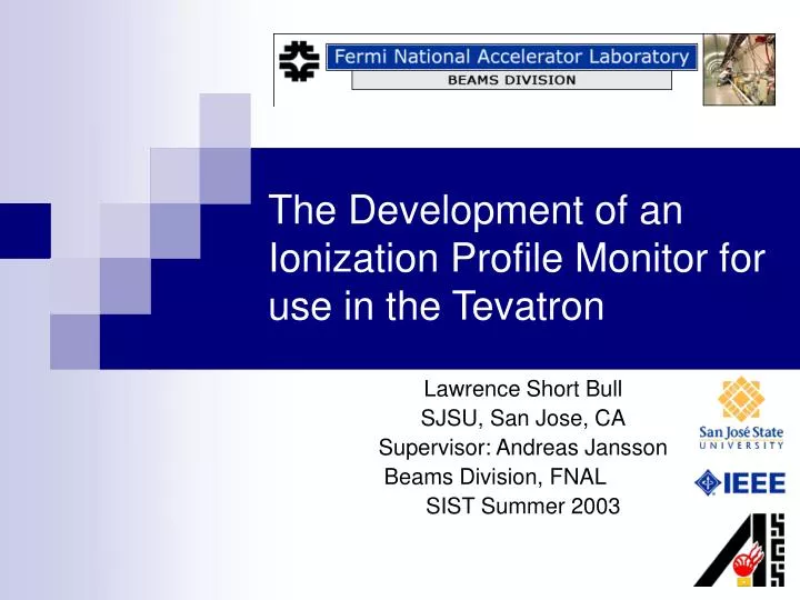
The Development of an Ionization Profile Monitor for use in the Tevatron. Lawrence Short Bull SJSU, San Jose, CA Supervisor: Andreas Jansson Beams Division, FNAL SIST Summer 2003. Agenda. Introduction Principles of Operation Design Details Experiments Conclusion

E N D
The Development of an Ionization Profile Monitor for use in the Tevatron Lawrence Short Bull SJSU, San Jose, CA Supervisor: Andreas Jansson Beams Division, FNAL SIST Summer 2003
Agenda • Introduction • Principles of Operation • Design Details • Experiments • Conclusion • Acknowledgements
Introduction • Quantities of Interest • Luminosity • Emittance • Emittance Monitoring Devices at FNAL • Flying Wire • Synchrotron Light Monitor • Ionization Profile Monitor (IPM)
Luminosity • Run II Goals: peak L 5.1E31 cm^-1sec^-1, integrated 2fb^-1
Emittance • projection onto x/y axis provides transverse beam dist. • r.m.s. value of beam density distribution provides measure of beam size • Beam size given as r.m.s of Gaussian beam profiles • Initial distribution not quite Gaussian, by time final energy reached is very good approximation.
Emittance monitoring in Tevatron • Flying Wires • Evasive diagnostic tool • Synchrotron Light Monitor • Non-evasive • Reported emittances show discrepancy • Potential emittance monitoring in Tev • IPM • Schottky Detector
Why an IPM for the Tev? • Run II Instrumentation Motivations • Transverse and longitudinal emittance preservation • Real time operational tuning & monitoring • Tev IPM provides turn-by-turn profile measurements for transverse injection matching • Sync lite only “on-line” transverse profile monitor available during store (insuff. Light @ 150 Gev)
IPM Fundamentals • Provide transverse beam profiles: vertical & horizontal • Residual gas ionization occurs with each bunch passage • Collection of ions/electrons with electric clearing field • Combat space charge effects • Utilizes microchannel plate(MCP) for charge multipliction • Amplified signal of charge collected on anode strip • Signal integrated, amplified, and digitized • Sent from memory to processor to provide histogram profiles
MCP fundamentals • Array of dynodes • Contain large number ~1E4-1E7 • Aspect ratio: 40-400 • Diameter: 5-25 microns • Intrinsic impedance: ~1E9ohm • Intrinsic capacitance: ~ 30pF • Gain: 1E4-1E7 • Gain degradation proportional to extracted charge
QIE ASIC • Charge, Integration, Encoding • Input current integrated over 4 ranges • Pipelined into 4 stages at 25nsec per stage • Output is 5 bit mantissa, 2 bit range exponent, 2 bit cap ID • in calibration mode the FADC is strictly linear with 32 linear counts @ 0.87 fC/count • Input charge: 6.1fC – 26fC
Tev IPM Design • 36 X 36 proton and pbar bunches • Time between bunches ~396ns • Bunch length ~ 3ns r.m.s., 18-20ns • Only ~1000 e liberated during ionization • Electronics must be low noise • Need Faraday screen to protect detector from image current @ 53MHz • Pull only signal through vacuum flange, reference terminated @ vacuum • Anode to ground completely floating Beam B E screen MCP Anode strips
Block diagram/data flow chart in tunnel in upstairs PC Pbar revolution marker Header card Timing card Proton revolution marker Injection event 53 MHz RF off-the-shelf To power supplies Sample clock (17.6 MHz) GPIB controller PCI BUS Header byte QIE mode QIE reset Kwame Vince, Mark et al QIE Data FPGA 16 (8 QIEs) optical driver serializer Fast (wide) memory Anode stirp signals (~128) PCIX bus DMA xfer Burst mode ~1 Gbit/s 16 serial links (optical fiber) ~1.6 Gbits/s/link ~23 Gbit/s total QIE
MI IPM Studies IMPM1H • Utilized IPMM1H & IPMM2H • Investigate effects of a varying bias voltage for MCP in detectors • ACNET variables I:HxMCPV, I:HxPMEM[ ] ,I:HxPMSG[ ] datalogged at node TevJA • Settings on LabView interface determine what turn number was datalogged • Two ranges were studied IPMM2H
QIE Noise Measurements • The noise floor of the CKM QTBB floor was determined • Noise for various cable configurations was to be determined QIE A Clock dist. ckt. 40MHz 16 bit SERDES w/ 8B/10B Data Multiplexing QIE B
Noise floor channel A: input impedance = 50 ohm Pedestal = 19.481 r.m.s = 0.6919
Noise floor per cap ID: input impedance = 50 ohm Cap ID 0 Cap ID 1 r.m.s = 0.6647 r.m.s = 0.6642 Cap ID 2 Cap ID 3 r.m.s = 0.6709 r.m.s = 0.6814
Determination of Gain Factor per cap ID: Zin = 50 ohm Gain factor for channel: 0.7579 Noise for channel: 3171e
Capacitance input to either signal or reference inputs Peculiar behavior displayed, further investigation required
Configuration of interest: input cap. To both signal & reference Noise levels appear within tolerances for design
Noise floor channel A: input impedance = 93 ohm Pedestal = 12.7432 r.m.s. = 0.6848 Similar results as 50 ohm case when individual cap id’s examined
Determination of Gain Factor per cap ID: Zin = 93 ohm Gain factor for channel: 0.7571 Noise for channel: 3123e Less noise, relatively the same gain factor for the channel than the 50 ohm setting
Cable Test Zin = 93 ohm • 100 ohm twisted pair cable connected to both signal and reference • Length of cable = 3.75 m • Shield of each cable connected • Return for each cable connected • Zin = 93 ohm, noise is 6,808 e • Zin = 50 ohm, noise is 10,844 e Zin = 50 ohm
Conclusion • Emittance as reported by IPM very sensitive to output current; N2 leak must be added with care, low gain MCP • MCP test stand will be used to study MCP properties for this project in addition to future projects. Also to diagnose MCP’s coming out of the machine • If QIE noise results correct, good thing. Seem slightly low. • Tev IPM up for technical DOE review in Oct., things look good and will more than likely be commissioned • Encouraging to see CMS & Beams Div. Collaborating on project • FNAL is a rocking place to work
Acknowledgements • I would like to thank Andreas Jansson, Claudio Rivetta, Hogan Nyugen, Jim Zagel, Kwamie Bowie, Dianne Engram, Elliot McCrory, Dr. Davenport and rest of SIST committee. • The 2003 SIST summer interns