Download
1 / 27
270 likes | 371 Views
Scintillator HCAL project overview. Felix Sefkow HCAL Main Meeting June 30, 2008. Where we are, where we go:. Analysis: status and opportunities Test beam at FNAL R&D, EUDET and beyond. From proof-of principle to reality. △ QGSP-BERT. □ LHEP. data. Validate shower models.

E N D
Scintillator HCAL project overview Felix Sefkow HCAL Main Meeting June 30, 2008
Where we are, where we go: • Analysis: status and opportunities • Test beam at FNAL • R&D, EUDET and beyond Project overview
From proof-of principle to reality Project overview
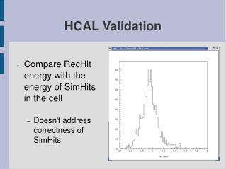
△QGSP-BERT □ LHEP data Validate shower models M.Thomson (Cambride) • Model uncertainties on PFLOW performance • Confront shower models with test beam data • First results on global properties • Next: fully exploit granularity for fine structure Project overview
Validate PFLOW performance • Test beam ‘jets’ would require magnet and tracker (future) • Jet energy resolution depends on hadronic energy resolution and confusion • High granularity, low occupancy: use event overlay techniques • Two particle separation in test beam data and Monte Carlo: CALICE preliminary A. Raspereza Project overview
Calibration procedures Talks by Sebastian, Shojun,Trygve • Non-linearity correction: test with electron data • MIP calibration: in test beam data, explore use of MIP segments in hadron showers • Correct for temperature-induced variations • Use T-sensors and measured T dependences • Use gain monitoring, adjust voltage Project overview
Analysis opportunities • Wonderful results - and there is so much more to do… • precision: model uncertainties ~ exp errors • 3d profiles, correlations, sub-structure • software compensation (weighting), ultimate resolution • temperature corrections applied • PFLOW: 2 part sep: more distances, energies, MC • Pandora-Tbeam • angular incidence, protons, low energies • ECAL HCAL combined: E res and PFLOW • new generation of PhD students, more institutes Project overview
Collaborating institutes • Czech R.: Prague • France: LAL Orsay • Germany: DESY, Hamburg, Heidelberg, MPI Munich, Wuppertal • Japan: Kobe, Shinshu • Russia: JINR; ITEP, LPI, MEPHI Moscow • UK: Cambridge, Imperial C, UCL, ,Manchester, RAL • US: Northern Illinois In preparation • Canada: McGill • Norway: Bergen Under discussion: • Italy: INFN Rome I Project overview
HCAL software • Reconstruction software and data base continuously improving • see talks by Niels and Andrea • data should be analyzable outside DESY - already now! • still a lot to do on spatial dimensions • tracking, alignment, shower centre, bias corrections,… • integrate with sci ECAL: reco, sim, digit • And later with DHCAL… • Maintain link to optimization studies • Core software: as much as possible and reasonable Project overview
New Mokka model • Revised, refined, realistic parameterization • New degrees of freedom • Detailed modelling of layer edges • Non-pointing cracks in rφ and z possible • End caps A. Lucaci, R. Diener (DESY) Project overview
Test beam at Fermilab • Preparation is everything! Project overview
CALICE@FNAL plans • Experience from May and plans for July • Low energies and good statistics for technology comparison • See talk by Erika • September: integration of SciECAL • Early next year: possibly 2nd all-scintillator run • Later in 2009: expect first set of DHCAL layers from US K.Gadow Project overview
R&D on scintillators and sensors Progress with photo-sensors: new options (?) • See talks by Roman, Simon • sensor on tile, with fibre: OK • Thinner scintillator possible with MRS-APD or MPPC • sensor on tile, direct coupling: ? • in principle possible with blue-sensitive sensors (MPPC, + ?) • Light yield OK for 5mm tiles, but non-uniform • 3mm tiles, non-uniformity compensation: needs larger area, new package • Strips: works in ECAL, LY and unif. OK but less advantageous for HCAL • sensor on PCB: studied at NIU, T2K electronics • issues: optical stability, integration chain Project overview
EUDET prototypes • The “integration prototype” • 2nd generation ASICs • electronics integration, c • calibration system, • compact mechanics • 2nd generation ASICs: • On-chip zero-suppression, digitization and TDC • SPIROC1: on the test bench since end 07 see Wei’s talk • some bugs (ADC ramp polarity, probe bus) and some mircales on analogue side • tests to expand on digital side with new test board • SPIROC2: submitted in June, expected in October Ludovic’s talk • "1st chip where everything works" • hopefully OK for EUDET, but possibly one more version needed • 3rd generation (beyond EUDET): • individual channel trigger handling • signal to noise for low gain sensors Project overview
EUDET, cont. • Calibration system: talks by Sebastian, Ivo • two approaches: electrical and optical distribution • both make progress, both have open issues • Electronics integration: tall by Mathias • First layer board (HBU): layout waiting for tile dimensions • Work on digital interface started • Prototyping sequence: • first proto: tile integration and readout chain 2008 • second proto: "real" readout board for cassette and end board 2009 • goal: a "demonstrator module" - 2m long, 7mm thin • possibility: new minical: 12 layers x 12x12 tiles • Absorber mechanics: talk by Kirsten • Detailed FEM calculations confirm design with minimal dead space and no gaps • 1st step layer demonstrator, 2nd step 1:1 model Project overview
Far future: DevDet • EU FP7 DevDet proposal submitted in Feb 08 • evaluated 12.5/15, but approval not very likely • Even without funding: we know what we want and will apply again • EUVIF: vertical integration facility • HCAL project: • 2nd generation prototype, compact • stainless steel absorber for tests with B>0 • scalable integration facilities • Eudet to be extended -> 2010, next FP7 call 2010 Project overview
Conclusion • Test beam data: a treasure • Ongoing data taking: needs your support • EUDET and beyond: focussed R&D • Enjoy the meeting! Project overview
Tile sensor systems with WLS fibre • Present test beam system • 5mm thick tile with fibre, MEPHI/ PULSAR SiPM, 15 pixels/MIP • Several new options: reduce to 3 mm thick tiles • Hamamatsu MPPC-1600 • MRS APDs (CPTA) M.Danilov (ITEP) Project overview
Tile 30x30x5 mm3 Tile sensor direct coupling • Possible with blue-sensitive sensors • Hamamatsu MPPC 1600 (400) • Obtain about 7 (11) px/MIP from 5 mm tiles; low noise • increase area • Need to restore uniformity • Some addal light cost • Other proven option: strips • CALICE SciW ECAL N.D’Ascenzo (DESY) 1600 px V.Zutshi (NIU) D.Jeans (Kobe) Project overview
V.Rusinov (ITEP) Tile PCB coupling • Scintillator photo-sensor system has to match electronics PCB tolerances • Several options • Mega-tiles (easier assembly, but some optical cross-talk • New: idea “lego” tiles with alignment pins • 30x30x3mm3 • Other option: surface-mounted sensors on PCB • Different integration chain SiPMs P.Rubinov (FNAL) Project overview
Reflector Foil 100µm Polyimide Foil 100µm HBU Interface 500µm gap ASIC TQFP-100 1mm high PCB 800µm Sector wall Top Plate 600µm steel Spacer 1.7mm Top Plate fixing Component Area: 900µm high HBU height: 6.1mm (4.9mm without covers => absorber) SiPM Bolt with inner M3 thread welded to bottom plate Bottom Plate 600µm Tile 3mm Absorber Plates (steel) Integrated layer design DESY M.Reinecke (DESY) integrated Project overview
Optical calibration system M.Reinecke (DESY) • SiPMs, MPPCs are self-calibrating • Ph.e. peak distance ~ gain • Embedded LEDs • electronic signal distribution • tested, no cross-talk to sensors seen • To be optimized: dynamic range, LED uniformity • Alternative: central driver and optical signal distribution S.Weber (Wuppertal) I.Polak (Prague) Project overview
0.1pF-1.5pF 1.5pF Slow Shaper Analog memory 50 -100ns Low gain Preamplifier Gain Gain selection Depth 16 Slow Shaper 0.1pF-1.5pF 12-bit Wilkinson ADC Charge measurement 15pF 50-100ns Depth 16 READ HOLD IN High gain Preamplifier Fast Shaper Conversion 80 µs Variable delay 15ns Discri Trigger Flag TDC 8-bit DAC 0-5V Depth 16 4-bit threshold adjustment DAC output Analog output Time measurement TDC ramp 300ns/5 µs 10-bit DAC Common to the 36 channels New ASIC on the test benches • Auto-triggering and time measurements • ADC and TDC integrated • Power pulsing, low (continuous) power DAC L.Raux (LAL) R.Fabbri (DESY) Project overview
AHCAL Slab 6 HBUs in a row HBU HCAL Base Unit 12 x 12 tiles SPIROC 4 on a HBU HEB HCAL Endcap Board Hosts mezzanine modules: DIF, CALIBand POWER HLD HCAL Layer Distributor Barrel HCAL architecture Front end ASICs embedded Interfaces accessible 1/16 of barrel half Power: 40 µW / channel Heat: T grad. 0.3K/2m Time constant: 6 d P.Goettlicher (DESY) Project overview
Interface Prototype Details M.Reinecke (DESY) Project overview
Mechanical structure • Aggressive design: 3mm walls • No additional spacers • FEM calculation with sector details for full barrel • Max displacement 2mm, stress • Integration with cryostat and ECAL K.Kschioneck (DESY) Project overview