Download
1 / 8
90 likes | 411 Views
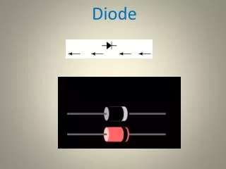
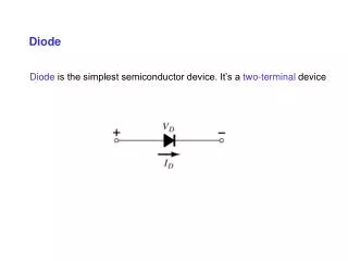
Semiconductor diode. A semiconductor device model. Introduction. The diode is the classical semiconductor device, and is mainly used as a rectifier From a modeling perspective the device has a well known theoretical behavior, so it often serves as a benchmark structure for device simulations

E N D
Semiconductor diode A semiconductor device model
Introduction • The diode is the classical semiconductor device, and is mainly used as a rectifier • From a modeling perspective the device has a well known theoretical behavior, so it often serves as a benchmark structure for device simulations • A simple implanted diode structure have been modeled in COMSOL Multiphysics, and analyzed using stationary and transient analysis • In particular, the electrical IV-characteristic, and the reverse recovery is studied
Model Definition – Geometry • The geometry is a cross-section of the diode, using depth of 1 µm of the implanted pn-junction
Model Definition – Equations • The Poisson equation is coupled with the drift-diffusion equations for electrons and holes: • Electrons and holes assume to have a Boltzmann distribution, which is an approximation for the Fermi-Dirac distribution • Shockley-Reed-Hall recombination is present inside the semiconductor
Model Definition – Mesh • The mesh have to be dense near the pn-junctions and in the transition between the lowly doped and highly doped n-type regions
Results • The electrical IV-characteristics can be used to extract the diode’s ideality factor, on-resistance, and saturation current
Results • A surface plot in log scale of the hole concentration reveals that the diode has entered high-level injection at 0.2 mA forward current
Results • The transient simulation studies the transition from the high-level injection state at forward bias to the blocked state in reverse bias • The diode reach a high reverse voltage with a high current, maximizing the risk of failure due to the large dissipated power