Download
1 / 17
170 likes | 173 Views
This summary provides an overview of the DEPFET power supply design, including details on channel configurations, noise distribution, load response tests, and development steps. The current status of development and production progress is also discussed.

E N D
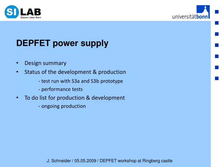
DEPFET power supply Design summary Status of the development & production - test run with S3a and S3b prototype - performance tests To do list for production & development - ongoing production J. Schneider / 05.05.2009 / DEPFET workshop at Ringberg castle
DEPFET power supply Design summary: DEPFET Power supply for lab measurements & TB runs ! • 20 individual supply channel • high voltage supply module • voltage and current measurement • remote control via USB • storage of all supply settings • output card defines purpose two prototypes are available - one for the S3a system - one for the S3b system (CERN - DEPFET TB at SPS - 2008)
DEPFET power supply Channel configurations: 0 to +25 V @ 0 - 20 mA source/sink 0 to -25 V @ 0 - 20 mA source/sink +/-15 V @ 0 - 20 mA source/sink 0 to +25 V @ 0 - 300 mA source 0 to -25 V @ 0 - 300 mA sink 0 to +25 V @ 0 - 300 mA sink 0 to -25 V @ 0 - 300 mA source 0 to +10 V @ 0 - 800 mA source OpAmp output stage (low current) Darlington output stage (high current) • channel configuration is independent of the others even on the same module • channels on same card share same GND • channels on different cards are insulated from each other • total output current of one quad supply module is limited to 300mA / 800mA
DAC DAC + - + - DEPFET power supply Channel configurations (principle): OpAmp output stage (low current) Darlington output stage (high current) Uout Uout
DEPFET power supply Noise Distribution: mean = 12,17 ; = 0,5 Common Mode: = 16,3 (Contribution from Simone Esch, Bonn) Test run with S3a-System:
DEPFET power supply Noise Distribution: mean = ~14,5 Common Mode: = ~16,8 (Contribution from Sergey Furletov, Bonn) Test run with S3b-System:
DEPFET power supply [V] [V] • linear behavior • slope due to the resistive component • of the conducting traces, connectors • and cables to the measurement • equipment • -> no regulation instability [mA] [A] Resistive load response test: Channel config: OpAmp output Channel config: Darlington output - linear behavior till the OpAmp output protection clamps the voltage -> no regulation instability
DEPFET power supply Capacitive load response test: • There is a need to do this test to see if regulation is stable -> we expect several capacitive loads on the hybrids -> The test with the DEPFET hybrids showed that the regulation is stable! but we do not know so far what is the safety margin
DEPFET power supply Load transient response for darlington output (high current): 35mA transient (positive) 35mA transient (negative) -> no regulation instability-> no regulation instability
DEPFET power supply Conditions: • 50 Ohm load • 50 cm coaxial cable • frequency band 160Hz – 58 MHz @ -3dB Result: -> max. 1,3mV RMS noise measured over hole frequency band Noise measurement for darlington output (high current):
DEPFET power supply Development steps and work packages: available prototype for S3a-System (CURO2/Switcher2) linearity / dynamic range / control deviation load tests (resistive, capacitive and dynamic) firmware debugging for the USB microcontroller performance tests S3a-prototype: stable operation with module adapting to the S3b-system - redesign hardware S3b-prototype: stable operation with module writing the application software S3b-prototype: final tests S3b series production finally 10 power supplies available for TB & lab measurements Status of the development & production progress: Sep. 2008 time scale now Summer 2009
DEPFET power supply • µC firmware needs still some extensions • HV module is tested but not fully debugged • capacitive load test -> more details • some development in the control software for TestBeam issues • series production of nine further supplies is ongoing -> backplanes -> quad cards -> HV modules -> output cards -> final assembly • Hardware available: (for nine further P.S.) • - cases • controller cards To do list for production & development :
DEPFET power supply • ... We are in time ... for TB 2009 … ... Questions so far? ...
many thanks … …
Digital isolators Digital isolators Digital isolators Digital isolators Digital isolators Digital isolators Quad channel supply module Quad channel supply module Quad channel supply module Quad channel supply module Single channel supply module Quad channel supply module DEPFET power supply Block diagram of the multi channel power supply: Analog voltage lines Digital control bus, 24 V supply backplane USB Interface & Microcontroller Display & switches Relay card D-Sub connector to DEPFET module HV module • 5 quad supply modules + 1 HV module • 21 supply voltages • each module has a floating ground • Controller • non volatile storage of voltage settings • USB interface (local control optional) • Relay card • controlled switching of the voltageoutputs Multi channel power supply in 15” case
. DAC DAC DAC current sense current sense current sense DEPFET power supply Quad supply module: Bus connector isolated power supply & filter Front panel 24 V DAC digital isolators EEPROM SPI programmable voltage source current sense ADC voltage sense output voltages • four independent programmable output voltages with common floating ground • voltage range: -25V … +25V • output current : • +/- 15 mA (OPA output) • max. 300 mA (power transistor, config. current limit & pol.) • voltage & current read back • EEPROM stores/restores voltage settings • optional front panel for local control Quad supply module card