Download
1 / 34
350 likes | 476 Views
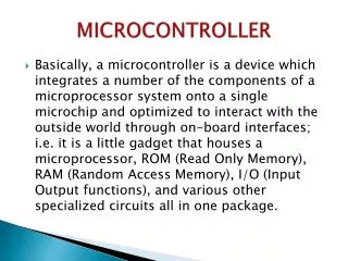
Microcontroller PARALLAX SX-28AC. Presented By: Muhammad Farhan Mughal. Key Features. 75 MIPS As low as 13.3 ns instruction cycle. RISC like architecture. EE/Flash rated for 10,000 times rewrite cycles. Eight level push/ pop hardware stack for subroutine operations.

E N D
Microcontroller PARALLAX SX-28AC Presented By: Muhammad Farhan Mughal.
Key Features • 75 MIPS • As low as 13.3 ns instruction cycle. • RISC like architecture. • EE/Flash rated for 10,000 times rewrite cycles. • Eight level push/ pop hardware stack for subroutine operations. • 2048 words EE/Flash program memory. • 136 x 8 bits SRAM data memory. • Fast and deterministic interrupts.
Key Features • Flexible I/O • All ports are individually accessible. • No need for pull-up resistors. • One 8-bit timer /counter with programmable 8-bit prescaler. • Watchdog timer. • Analogue comparator. • Brown-out detector. • Power- on reset. • 28-pin package.
Applications • The SX may be used as a solution for process controllers. • Electronic appliances tools. • Security monitoring systems. • Sound and signal generation. • GPS interface. • Robotic control. • Motor control. • Applications such as interactive toys, infrared decoders, and other timing-sensitive projects are also common with the SX.
Ports Description PORTA • It is a 4-bit I/O port. • Locating at memory address 05h. • Each port has three associated registers to configure each port pin as I/O ,TTL or CMOS level and to enable/disable weak pull up resistors. • To access these registers value must be written into the MODE register.
PORT COFIGURTAIONS Data direction Registers RA,RB,RC TTL/CMOS Selected Registers LVLA,LVLB, LVLC Pull-up Enable Registers PLPA, PLPB, PLPC 0 1 0 1 0 1 INPUT OUTPUT CMOS T T L ENABLE DISABLE
Port B and Port C • They are similar to port A just differ by they both are 8-bit registers. • Port C can only be used as I/O but Port B can be used for interrupts and comparator functions.
MODE REGISTER • The MODE register controls access to the port configuration registers. • It is accessed by the following special purpose instructions: • mov M, #lit (move literal to MODE register). • mov M,W (move W to MODE register). • mov W,M (move MODE register to W).
How to program a pull-up resistor • mov M,#$0E ; MODE=0Eh to access port pull-up ; registers • mov W,#$03 ; W = 0000 0011 • mov !RA,W ; disable pullups for RA0 and RA1 • mov W,#$FF ; W = 1111 1111 • mov !RB,W ; disable all pullups for RB0-RB7 • mov W,#$00 ; W = 0000 0000 • mov !RC,W ; enable all pullups for RC0-RC7
Status Register C = Carry Flag DC = Digital or auxiliary carry Z= zero flag PD = Power down TO = Time out
Option Register RTW = RTCC/W Use real time SFR or W register. 0 = W 1 = RTCC RTW_IE = RTCC interrupt RTW_IE = 0 => Interrupt Enable RTW_IE = 1 => Interrupt Disable
Option Register • RTS = RTCC increment select 0 = RTCC increments on internal instruction Cycle. 1 = RTCC increments upon transition on RTCC pin. • RTE_ES RTCC edge select: 0 = RTCC increments on low-to-high transitions. 1 = RTCC increments on high-to-low transitions. • PSA Prescaler Assignment: 0 = Prescaler is assigned to RTCC, with divide rate determined by PS0-PS2 bits 1 = Prescaler is assigned to WDT, and divide rate on RTCC is 1:1
Option Register • PS2 – PS0 (Prescaler divider)
Memory Organization • PROGRAM MEMORY:- • The program memory is organized as 2K, 12-bit wide words. • The program counter starts at zero. • PROGRAM COUNTER:- • The program counter contains the 11-bit address of the instruction to be executed. • The lower 8-bit of the program counter are contained in the PC register while the upper bits come from the upper three bits of status register (PA0,PA1,PA2).
Memory Organization • Subroutine Stack:- • The subroutine stack consists of eight 11-bits save registers. • The stack is physically and logically separated from the data RAM. • The program cannot read or write stack. • DATA MEMORY :- • The data memory consists of 136 bytes of RAM. • Can be accessed directly or indirectly using FSR register.
Memory Organization • FILE SELECT REGISTER:- • FSR can be used to access RAM locations. • an example of how to write to register 10h in Bank 4: • mov FSR,#$90 ;Select Bank 4 by ;setting FSR<7:5> • mov $10,#$64 ;load register 10h with ;the literal 64h
Interrupt Support • The device supports both internal and external maskable interrupts. The internal interrupt is generated as a result of the RTCC rolling over from 0FFh to 00h. This interrupt source has an associated enable bit located in the OPTION register. • Port B provides the source for eight external software selectable, edge sensitive interrupts. • The WKEN_B register allows interrupt from Port B to be individually enabled or disabled.
Instruction Set Features • All single-word (12-bit) instructions for compact code efficiency. • All instructions are single cycle except the jump type instructions (JMP, CALL) and failed test instructions (DECSZ fr, INCSZ fr, SB bit, SNB bit) which are two cycle. • Bit manipulation instructions (Set, Clear, Test and Skip if Set, Test and Skip if Clear). • Many instructions include a destination bit which selects either the register file or the accumulator as the destination for the result.
Instruction Set Features • Bit manipulation instructions (Set, Clear, Test and Skip if Set, Test and Skip if Clear). • Indirect addressing data pointer FSR (file select register) memory-mapped as a register file. • Eight-level, 11-bit push/pop hardware stack for subroutine linkage using the Call and Return instructions.
Instruction Set • LOGICAL OPERANDS:- Mnemonic, Operands Description Clock Cycles AND fr,W AND of fr and W into fr (fr = fr & W) 1 AND W,fr AND of W and fr into W (W = W & fr) 1 AND W,#lit AND of W and Literal into W (W = W &b lit) 1 NOT fr Complement of fr into fr (fr = fr ^ FFh) 1
Logical Instructions Mnemonic, Operands Description Clock Cycles OR fr,W OR of fr and W into fr (fr = fr | W) 1 OR W,fr OR of W and fr in to fr (W – W | fr) 1 OR w,#lit Or of W and Literal into W (W = W | lit) 1 XOR fr,W XOR of fr and W into fr (fr = fr ^ W) 1
Thank You. TAKE CARE.