Download
1 / 14
150 likes | 160 Views
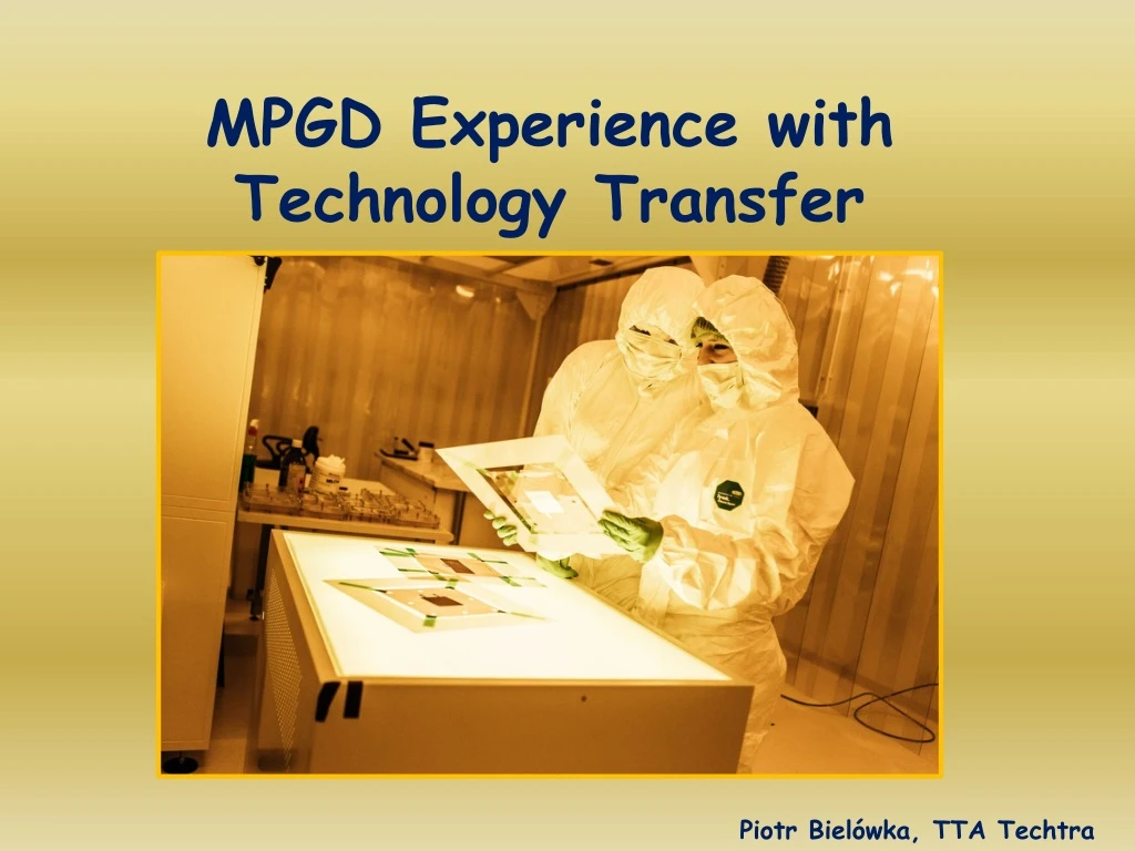
MPGD Experience with Technology Transfer. Piotr Bielówka, TTA T echtra. 1. History. Technology Transfer Step 1: Legal issue Licence for Micro- Chemical - Vias - for „ kapton etching ” technology in PCB Licence for Microvia technology - for internal GEM R&D

E N D
MPGD Experience with Technology Transfer Piotr Bielówka, TTA Techtra
1. History Technology Transfer Step 1: Legalissue Licence for Micro-Chemical-Vias - for „kaptonetching” technology in PCB Licence for Microviatechnology - for internal GEM R&D License for Manufacturing and Commercialisation of Gem Foils and Gem-based products Workshop in Bari, 2019
Technology Transfer Step 2: Cooperation with existingindustry Eldos – PCB producer Techtra was responsible for Kaptonetching Eldos was responsible for alltherest Problems:- itishard to separateproductionsteps especialyduringR&D! - productionregime of big PCB producer Benefits for Techtra: - „experience transfer” fromEldos to Techtra Workshop in Bari, 2019
Technology Transfer Step 3: Startingthe business Techtra decides to assemblewhole GEM productionline. The machinery was installedin Wrocław Technology Park. Techtra getUE supportwithin „IntelligentDevelopment” project. We had 2 rooms of about 50m2. Laboratory scale workshop to have everything under control. Workshop in Bari, 2019
Technology Transfer Step 3: Starting the business Techtra gained production capacity in 2009, with followingrestrictions: • Uniformitylimited to about 10x10cm2 • Max yield of around 70% due to lack of cleanroom, others? Workshop in Bari, 2019
Technology Transfer Step 4: Full scaletechnologyimplementation with dedicatedinfrastructure for GEMs Room 1:cleanroom, lamination and exposure Room 1 – 48 m2 Room 2 – 48 m2 Room 3 – 96 m2 Total – 192 m2 Room 2:resist development Room 3b: Kaptonetcher Room 3a: Cu etcher Workshop in Bari, 2019
Technology Transfer Step 4: Dedicatedinfrastructure for GEMswerebased on CERN experience. The choice of machines and workshop layout wereconsulted with Rui. Machineswereproduced by „Wise” company, Parma. New developer New Cuetcher Olddevelopingand etching set Workshop in Bari, 2019
Machinery„dedicated” for GEM production Techtra Techtra isfocused on GEM foilsand GEM detectormanufacturing. All machines have been tunedfor GEMproduction. Cleanroom Oldexposure unit New exposure unit Workshop in Bari, 2019
Technology Transfer Step 5: Quolitycontrol: defineparameters! • Leakagecurrentbelow 1nA@100cm2 @600V @30 %HR HV testing stand Workshop in Bari, 2019
Technology Transfer Step 6: Look for newapplications: Techtra is the only commercial producer of GEM detectors Commerciallyavailableproduct Design and prototyping Workshop in Bari, 2019
2. Techtra’scompetences • Techtra hasmasteredalltechniques for GEMsproduction: • Copperetching on thincopperlayers with precision of +/- 2um • Kaptonetching in kaptonlayerwith precision of +/- 2um at „double” and „single masktechnique:” • 3. Dedicatedelectronicreadout for detectors: Workshop in Bari, 2019
4. Validationdetectorswith small X-raytube: • 5. We areparticipating in few UE projects. • We are very willing to cooperate in R&D and commercialization for ResistiveCoatings for Gaseous Detectors. Workshop in Bari, 2019
Summary: • Technology Transfer issues: • Legalissuesarecritical for companies . Thatneedstime ! • Production chain: techniques (MCV….), consumables ( Kapton, DLC coating…), transport, validationand installation. • Tuning a collaboration with PCB Industry needs time, ifyouneedkaptonetchingtechnologyyoucan: • do a technology transfer • start a cooperation with: CERN, Techtra, Mecaro, TechEtch, Micropack… • Find an additional applications of your device • Look for externalfunding……… everythingcostsmorethanyouexpect Workshop in Bari, 2019
Our Core GEM-team Project numer: POIR.01.01.01-00-0192/16 TTA TECHTRA Sp. z o.o. ul. Dunska 13phone: +48 71 798 58 8554-427Wroclaw www.techtra.plPoland e-mail: techtra@techtra.pl Workshop in Bari, 2019