Download
1 / 20
200 likes | 331 Views
High magnetic field studies of the fully gapped charge-density wave system (Per) 2 M (mnt) 2 (where M = Au and Pt). Ross D. McDonald , P.A. Goddard, N. Harrison, A. Migliori , A. Silhanek and J. Singleton National High Magnetic Field Laboratory, Los Alamos National Lab. A. Bangura

E N D
High magnetic field studies of the fully gapped charge-density wave system (Per)2M(mnt)2(where M = Au and Pt). Ross D. McDonald, P.A. Goddard, N. Harrison, A. Migliori, A. Silhanek and J. Singleton National High Magnetic Field Laboratory, Los Alamos National Lab. A. Bangura University of Oxford / University of Bristol. E. Akhadov, M.A Hoffbauer Chemistry Division, Los Alamos National Lab. A.P. Ramirez and X. Chi Bell Laboratories, Lucent Technologies.
Contents • (Per)2M(mnt)2, a low transition temperature fully gapped charge-density wave (CDW) system. • Application of high magnetic fields and the Pauli paramagnetic limit. • What state exists at fields exceeding the Pauli paramagnetic limit? • Extracting the gap from magnetotransport. • Model for the thermodynamic gap that includes interchain bandwidth. • Reentrant CDW behavior in the M = Pt compound. • Narrow band noise measurements and current/voltage oscillations. • Conclusion & possible phase diagram. • CDW-FET: quantum coherent switching.
- M(mnt)2 A highly 1D metal @ room temperature: Per2M(mnt)2. M = Au (s = 0) or Pt (S = 1/2) 3/4 full bands a = 16.6 Å b = 4.2 Å c = 26.5 Å = 94.5° 4 perylene molecules/unit cell 4 bands cross EF E. Canadell et. al. Eur.Phys.J.B42, 453 (2004)
Charge-density wave formation. • 3/4 full band is unstable to tetramerization of the perylene chains (CDW) • + Simultainious dimerization of the Pt(mnt)2 chains (spin Peierls) M = Au: TCDW = 12 K M = Pt: TCDW = 8 K CDW gap vs interchain bandwidth
Possible contributions to the conductivity. • Thermally excited quasi-particles (Ohmic and activated) • CDW de-pinning (non-Ohmic above a threshold field ET) • Residual sections of Fermi-surface (Metallic) CDW Not CDW Can use temperature and current dependence to distinguish contributions.
Charge-density waves in high magnetic fields: the Pauli paramagnetic limit. The Pauli Paramagnetic limit (BP): Free energy of the normal metal = Free energy of the CDW. F cannot reside in the gap () Insulator metal transition? Zeeman splitting CDW gap
Exceeding the Pauli paramagnetic limit. This indicates survival of the CDW above the Pauli paramagnetic limit. Per2Au(mnt)2: BP ≈ 37 T for = 6. Consistent with an inhomogeneous CDW phase Insulator insulator transition. Non-linear transport @ B > BP @ low temperatures.
Field-modulated CDW phase. Analogous to the Fulde-Ferrell-Larkin-Ovchinnikov phase of superconductivity. Spatially varying order parameter New long-period spatially modulated phase
‘Reentrant’ phases in Per2Pt(mnt)2. • Lower Pauli paramagnetic limit that the Au compound • But what is the origin of the high field increase in Resistance? Is the structure due to FICDWs? (i.e.Orbital physics)
Thermodynamic gap Remembering that in zero field the thermodynamic gap is the CDW gap minus the interchain bandwidth:
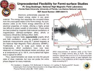
Modeling the gap and band parameters. Competition between Landau quantization opening and Zeeman splitting closing. non-parabolicity (B) from equating constant energy orbit with Onsager k-space area of the l = 0 Landau level. When no more orbital effects: 50me 0.01me
Please mind the gap. Gradient of Arrhenius plot yields activation gap How do the other contributions to and g(T)effect this? Mean field like? For Only negleible for T<1/2TCDW and small jy. 5% error in evaluating g over this temperature range and at low current. (N.B. 200% error @ 0.7 Tc)
Temperature and current dependent magnetotransport data Contours of constant power and resistance. Ohmic Negative differential resistance. Arrhenius plots to evaluate the activation gap. (T < 1/3Tc)
Gap data. Fit to 3-free parameters: (B), 4ta, vF • 4.02 meV (@ B=0) 0.8 meV 1.7 105 ms-1 • Good agreement with band calculations. BL=17 T E. Canadell et. al. Eur.Phys.J.B42, 453 (2004) Orbital effects irrelevant above BL Complex behavior due to stronger coupling to the lattice (Pt-spins) Saturation of magnetization
= 4b Narrow-band noise. Coherent de-pinning and re-pinning of the CDW: jCDW = nCDWevD Voltage noise at a frequency proportional to current (+harmonics) • Can this be used to measure (B)? “Perhaps the most spectacular measurement of a charge density wave material is the detection of current oscillations in the nonlinear conductivity region”- G Gruner, Rev. Mod. Phys., 60, 1129-1181 (1988).
Voltage oscillation data. Per2Pt(mnt)2: strong coupling of the CDW to the lattice + negative differential resistance Feedback to drive oscillations. T = 1.9 K Frequency diverges as the gap closes. Sample X-section ≈ 100x100mm. Band structure predicts 3.2x1021 cm-3
Summary & possible phase diagram. Spin Peierls ‘in competition’ with CDW (lowering transition temperature) As field polarizes localized Pt spins larger gapped CDW wins out over incommensurate CDW + Spin Peierls. Observed structure due to change in pinning?
Field effect CDW transistors. E-field perturbation of CDW: (Not just charge injection) Goal pattern the gate so as to achieve an spatial E-field modulation on a length scale comparable to the CDW period. Prototype devices. PMMA substrate and gate ~ 500 nm thick ~5% T = 4.2 K • Small perturbation in real space can have a large effect in k-space possibility of low power consumption. • Perturbation of coherent ground state possibility of fast switching.
Thanks P.A. Goddard, N. Harrison, Migliori, A. Silhanek, J. Singleton National High Magnetic Field Laboratory, Los Alamos National Lab. A. Ardavan University of Oxford. A. Bangura University of Bristol. E. Akhadov, M.A Hoffbauer Chemistry Division, Los Alamos National Lab. A.P. Ramirez X. Chi Bell Laboratories, Lucent Technologies. L. Balicas National High Magnetic Field Laboratory, M. Almeida Dep. Quimica, ITN, Portual. The Organizers