Download
1 / 1
20 likes | 267 Views
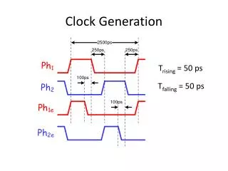
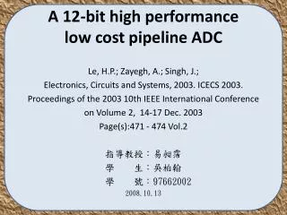
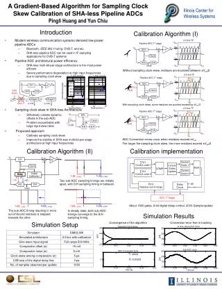
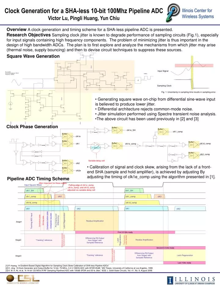
200uA. AC-coupled Differential Amplitude: 750mV Frequency: 200Mhz. 100Mhz. ÷2. 300uA. clk1e_SH. clk1_comp. Buffer. Buffer. Buffer. Buffer. Buffer. Buffer. Buffer. Buffer. Buffer. clk1e. clk1d_comp. clk1. clk1e_comp. clk3_comp. clk2. clk2e. Input Square Wave. clk1_SH.

E N D
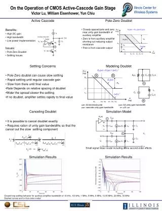
200uA AC-coupled Differential Amplitude: 750mV Frequency: 200Mhz 100Mhz ÷2 300uA clk1e_SH clk1_comp Buffer Buffer Buffer Buffer Buffer Buffer Buffer Buffer Buffer clk1e clk1d_comp clk1 clk1e_comp clk3_comp clk2 clk2e Input Square Wave clk1_SH clk1_SH clk3 clk3 clk1_comp clk1_comp clk1d_comp clk1d_comp clk2 clk1 clk1 clk2 clk2 Pre-Amping and Differencing Latch Regeneration Comparator bottom plate S/H top plate S/H bottom plate Comparator top plate Residue Amplification Tracking ADC Input Thermometer code lateched Stage1 First 3.5 bits ready Differencing RA Output from Stage1 with Sampled Reference Latch Regeneration Thermometer code latched Reference sampled by bottom plate Residue Amplification Stage2 “Tracking” reference Second 3.5 bits ready Differencing RA Output from Stage2 with Sampled Reference Reference sampled by bottom plate “Tracking” reference Latch Regeneration Stage3 Last 4 bits ready Clock Generation for a SHA-less 10-bit 100Mhz Pipeline ADC Victor Lu, Pingli Huang, Yun Chiu Illinois Center for Wireless Systems OverviewA clock generation and timing scheme for a SHA-less pipeline ADC is presented. Research ObjectivesSampling clock jitter is known to degrade performance of sampling circuits (Fig.1), especially for input signals containing high frequency components. The problem of minimizing jitter is thus important in the design of high bandwidth ADCs. The plan is to first explore and analyze the mechanisms from which jitter may arise (thermal noise, supply bouncing) and then to devise circuit techniques to suppress these sources. Square Wave Generation Input Signal Sampling Clock Fig. 1: Uncertainty in sampling time results in sampling error. • Generating square wave on-chip from differential sine-wave input is believed to produce lower jitter. • Differential architecture rejects common-mode noise. • Jitter simulation performed using Spectre transient noise analysis. • The above circuit has been used previously in [2] and [3] 25uA 25uA 100uA 25uA Clock Phase Generation 25uA Variable delay cell • Calibration of signal and clock skew, arising from the lack of a front-end SHA (sample and hold amplifier), is achieved by adjusting By adjusting the timing of clk1e_comp using the algorithm presented in [1]. Pipeline ADC Timing Scheme Jitter important for these edges Falling edge of clk1e_comp, clk1e_comp, and clk1d_comp adjusted via variable delay cell [1] P. Huang, “A Gradient-Based Digital Algorithm for Sampling Clock Skew Calibration of SHA-less Pipeline ADCs” [2] C. Jing, “A Clock Generator and Output Buffer for 12-bit, 75-MS/s, 3.3-V CMOS ADC with SFDR 85dB,” MS Thesis, University of California at Los Angeles, 1999 [3] A. M. A. Ali, et al, “A 14-bit 125 MS/s IF/RF Sampling Pipelined ADC with 100dB SFDR and 50 fs Jitter,” IEEE J. Solid-State Circuits, Vol. 41, No. 8, August 2006