Download
1 / 31
380 likes | 1.82k Views
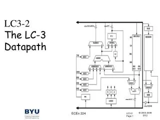
enaMARM. enaPC. PC. B. A. ALU. IR. enaALU. enaMDR. LC3-2 The LC-3 Datapath. Datapath Strategy. Take datapath elements one-by-one Determine how each works Clearly identify inputs/outputs and needed control Design the element When all done, doing control is straightforward…

E N D
enaMARM enaPC PC B A ALU IR enaALU enaMDR LC3-2The LC-3 Datapath ECEn 224
Datapath Strategy • Take datapath elements one-by-one • Determine how each works • Clearly identify inputs/outputs and needed control • Design the element • When all done, doing control is straightforward… • Push all the complexity into the datapath that we can ECEn/CS 224
The Bus enaMARM enaPC PC B A ALU IR enaALU enaMDR • Four major drivers: MARMUX, PC, ALU, MDR • It is the means of data transfer between units. ECEn/CS 224
Tri-State Drivers enaMARM enaPC PC B A ALU IR enaALU enaMDR module ts_driver ( din, dout, en ); input [15:0] din; output [15:0] dout; input en; assign dout = en ? din : 16’hZZZZ; endmodule 16 16 dout din en din[n] dout[n] en ECEn/CS 224
More Tri-State • Lots of drivers and lots of listeners • Only one driver on at any time • It’s a distributed MUX! Be careful! If more than one driver is on at once there will be contention on the bus with unpredictable results MARMUX MDR enaMARM enaMDR PC ALU enaPC enaALU Bus ECEn/CS 224
Typical Tri-State Drivers din dout en din dout t ECEn/CS 224
The Effective Address Block enaMARM enaPC PC B A ALU IR enaALU enaMDR • An adder, two muxes, and three sign extenders • Signals: IR[10:0] Ra[15:0] PC[15:0] selEAB1 selEAB2[1:0] eabOut[15:0] selMAR - – selEAB1 selEAB2 – ECEn/CS 224
The Effective Address Block Why are there 3 different sign extenders? LD 0 0 1 0 DR PCoffset9 LDR 0 1 1 0 Offset6 DR BaseR 0 1 1 0 JSR 1 PCoffset11 ECEn/CS 224
Designing the EAB eabOut[15:0] IR[10:0] Ra[15:0] EAB PC[15:0] selEAB1 selEAB2[1:0] ECEn/CS 224
The MARMUX enaMARM enaPC PC B A ALU IR enaALU enaMDR • Simply a MUX and a zero extender • Signals: IR[7:0] eabOut[15:0] selMAR MARMUXOut[15:0] selMAR – ECEn/CS 224
Designing the MARMUX MARMUXOut[15:0] IR[7:0] eabOut[15:0] MARMUX selMAR ECEn/CS 224
The PC enaMARM enaPC PC B A ALU IR enaALU enaMDR • A register, MUX, and an incrementer • Signals: clk reset selPC[1:0] eabOut[15:0] ldPC PCOut[15:0] Buss[15:0] – ldPC – selPC ECEn/CS 224
Designing the PC Buss[15:0] clk reset PCOut[15:0] ldPC PC eabOut[15:0] selPC[1:0] NOTE: Be sure your PC initializes to 0 on a global reset ECEn/CS 224
The IR enaMARM enaPC PC B A ALU IR enaALU enaMDR • Simply a loadable register, loads from bus when enabled for loading • Signals: clk reset ldIR Buss[15:0] IR[15:0] – ldIR ECEn/CS 224
Designing the IR IR[15:0] clk reset IR ldIR Buss[15:0] ECEn/CS 224
The nzp Flags enaMARM enaPC PC B A ALU IR enaALU enaMDR • Loadable registers which contain flags. • Load on some reg writes • Decode bus to determine flag values • Signals: clk reset flagWE Buss[15:0] N Z P – flagWE ECEn/CS 224
Designing the nzp Flags N Z P clk NZP reset flagWE Buss[15:0] How many of N, Z, P can be high at one time? ECEn/CS 224
The ALU enaMARM enaPC PC B A ALU IR enaALU enaMDR • Has 4 functions: add, and, not, pass • One operand always comes from regfile, other from mux • Signals: Ra[15:0] Rb[15:0] IR[4:0] IR[5] aluControl[1:0] aluOut[15:0] Rb – Ra – IR[5] – aluControl – ECEn/CS 224
The Operate Instructions ECEn/CS 224
Designing the ALU Rb[15:0] Ra[15:0] IR[4:0] IR[5] ALU aluControl[1:0] aluOut[15:0] ECEn/CS 224
The Memory enaMARM enaPC PC memWE ldMAR ldMDR B A ALU selMDR IR enaALU enaMDR • Writes on clock edge when memWE=1 • Data read from and written to memory passes through MDR • The MDRMUX controls where data is loaded from • Signals: clk reset selMDR ldMAR memWE ldMDR Buss[15:0] mdrOut[15:0] ECEn/CS 224
Designing the Memory Buss[15:0] clk reset ldMDR Memory ldMAR memWE selMDR mdrOut[15:0] ECEn/CS 224
The Register File enaMARM enaPC PC B A ALU IR enaALU enaMDR • Triple-ported memory (2 read ports, 1 write port) • Synchronous write, asynchronous read • Signals: clk reset regWE DR[2:0] SR1[2:0] SR2[2:0] Ra[15:0] Rb[15:0] Buss[15:0] (regWE) Rb Ra ECEn/CS 224
Register File Signals • DRis either“111”(subroutine call) or comes from IR[11:9] • SR2is alwaysIR[2:0] • SR1changes depending on the instruction • IR[11:9]onSTI, ST • IR[11:9]in one state associated withSTR • “111”onRET(same asIR[8:6]) • IR[8:6]otherwise • regWEis generated bythe control block ECEn/CS 224
LC-3 Instructions ECEn/CS 224
Building the Register File Buss[15:0] clk reset regWE RegFile DR[2:0] SR1[2:0] SR2[2:0] Rb[15:0] Ra[15:0] ECEn/CS 224
Building the Register File Reg0 Write Decoder Reg1 Reg2 Reg3 Register write signals Reg A 8:1 MUX Reg4 Reg B Reg5 Reg6 Reg7 DR[2:0] WE D[15:0] (Buss) CLK SR2 SR1 ECEn/CS 224
Building the Machine • Each element of the datapath can be considered independently, designed independently, and debugged independently • Once this has been done the control can be easily completed ECEn/CS 224
The LC-3 flagWE ECEn/CS 224
The LC-3 flagWE ECEn/CS 224
LC3 Controller LC3 Datapath IR N,Z,P Programmed Memory Control Signals ECEn/CS 224