Download

1 / 40
510 likes | 1.51k Views
8086 & Z80 µP. Lec note 2. Outline. Microprocessors History Data width 8086 vs 8088 8086 pin description Z80 Pin description. Microprocessors. Microprocessors come in all kinds of varieties from the very simple to the very complex

E N D
8086 & Z80 µP Lec note 2
Outline • Microprocessors • History • Data width • 8086 vs 8088 • 8086 pin description • Z80 Pin description
Microprocessors • Microprocessors come in all kinds of varieties from the very simple to the very complex • Depend on data bus and register and ALU width µP could be 4-bit , 8-bit , 16-bit, 32-bit , 64-bit • We will discuss two sample of it • Z80 as an 8-bit µP • and 8086/88 as an 16-bit µP • All µPs have • Address bus • Data bus • Control Signals: RD, WR, CLK , RST, INT, . . .
Internal and External Bus • Internal bus is a pathway for data transfer between registers and ALU in the µPs • External bus is available externally to connect to RAM, ROM and I/O • Int. and Ext. Bus width may be different • For example • In 8088 Int. Bus is 16-bit , Ext. bus is 8-bit • In 8086 Int. Bus is 16-bit , Ext. bus is 16-bit
8086 vs 8088 Only external bus of 8088 is 8_bit 8_bit Data Bus 20_bit Address 16_bit Data Bus 20_bit Address 8088 8086
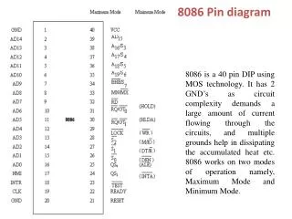
8086 Pin Description Vcc (pin 40) : Power Gnd (pin 1 and 20) : Ground AD0..AD7 , A8..A15 , A19/S6, A18/S5, A17/S4, A16/S3 : 20 -bit Address Bus MN/MX’ (input) : Indicates Operating mode READY (input , Active High) : take µP to wait state CLK (input) : Provides basic timing for the processor RESET (input, Active High) : At least 4 clock cycles Causes the µP immediately terminate its present activity. TEST’ (input , Active Low) : Connect this to HIGH HOLD (input , Active High) : Connect this to LOW (BR) HLDA (output , Active High) : Hold Ack (BG) INTR (input , Active High) : Interrupt request INTA’ (output , Active Low) : Interrupt Acknowledge NMI (input , Active High) : Non-maskable interrupt
8086 Pin Description DEN’ (output) : Data Enable. It is LOW when processor wants to receive data or processor is giving out data (to74245) DT/R’ (output) : Data Transmit/Receive. WhenHigh, data from µP to memory When Low, data is from memory to µP (to74245 dir) IO/M’ (output) : If High µP access I/O Device. If Low µP access memory RD’ (output) : When Low, µP is performing a read operation WR’ (output) : When Low, µP is performing a write operation ALE (output) : Address Latch Enable , Active High Provided by µP to latch address When HIGH, µP is using AD0..AD7, A19/S6, A18/S5, A17/S4, A16/S3 as address lines
Z80 Pin Description A15-A0 : Address bus (output, active high, 3-state). Used for accessing the memory and I/O ports During the refresh cycle the I is put on this bus. D7-D0 : Data Bus (input/output, active high, 3-state). Used for data exchanges with memory, I/O and interrupts. RD: Read (output, active Low, 3-state) indicates that the CPU wants to read data from memory or I/O WR: Write (output, active Low, 3-state) indicates that the CPU data bus holds valid data to be stored at the addressed memory or I/O location.
Z80 Pin Description MREQ Memory Request (output, active Low, 3-state). Indicates memory read/write operation. See M1 IORQ Input/Output Request(output,active Low,3-state) Indicates I/O read/write operation. See M1 M1 Machine Cycle One (output, active Low). Together with MREQ indicatesopcode fetch cycle Together with IORQ indicates an Int Ack cycle RFSH Refresh (output, active Low). Together with MREQ indicates refresh cycle. Lower 7-bits address is refresh address to DRAM
Z80 Pin Description • INT’ • Interrupt Request (input, active Low). • generated by I/O devices. • Checked at the end of current instruction • If flip-flop (IFF) is enabled. • NMI’ • Non-Maskable Interrupt • (Input, negative edge-triggered). • Checkedat the end of current Instruction • Higher priority than INT. • Independent from IFF Status • Forces CPU restart at 0066H.
Z80 Pin Description • BUSREQ’ • Bus Request (input, active Low). • higher priority than NMI • recognized at the end of current machine cycle • forces the CPU address bus, data bus, and MREQ, IORQ, RD, and WR to high-imp. • BUSACK’ • Bus Acknowledge (output, active Low) • indicates to the requesting device that address, data, and control signals have entered their high-impedance states.
Z80 Pin Description • RESET’ • Reset (input, active Low). • Must be active for three clock cycles • Initializes the CPU as follows: • Resets the IFF • Clears the PC and I and R • Sets the interrupt to Mode 0 • During reset time: • address and data go high-impedance • all control (out) signals go inactive state
Register Set • A :Accumulator Register • F : Flag register • Two sets of six general-purpose registers • may be used as 8-bit A F B C D E H L (A’ F’ B’ C’ D’ E’ H’ L’) • or in pairs as 16-bit AF BC DE HL (AF’ BC’ DE’ HL’) • The Alternative registers (A’ F’ B’ C’ D’ E’ H’ L’) not visible to the programmer but can access via: • EXX (BC)<->(BC') , (DE)<->(DE') , (HL)<->(HL') • EX AF, AF ’ (AF)<->(AF') what is this instruction useful for?
Register Set(cont) • 4 (16-bit) registers hold memory address (pointers) • indexregisters (IX) and (IY) are 16-bit memory pointers • 16 bit stackpointer (SP) • Program counter (PC) • Program counter (PC) • PC points to the next opcode to be fetched from ROM • when the µP places an address on the address bus to fetch the byte from memory, it then increments the program counter by one to the next location • Special purpose registers • I : Interrupt vector register. • R : memory Refresh register
Flag Register S Sign Flag (1:negativ)* Z Zero Flag (1:Zero) H Half Carry Flag (1: Carry from Bit 3 to Bit 4)** P Parity Flag (1: Even) V Overflow Flag (1:Overflow)* N Operation Flag (1:previous Operation was subtraction)** C Carry Flag (1: Carry from Bit n-1 to Bit n,with n length of operand) *: 2-complement number representation **: used in DAA-operation for BCD-arithmetic
DAA - Decimal Adjust Accumulator Adjusts the content of the Accumulator A for BCD addition and subtraction operations such as ADD, ADC, SUB, SBC, and NEG according to the table:
Instruction cycles, machine cyclesand “T-states” • Instruction cycle is the time taken to complete the execution of an instruction • Machine cycle is defined as the time required to complete one operation of accessing memory, accessing IO, etc. • T-state = 1/f (f:Z80 Clock Frequency) • f= 4MHZ T-state=0.25 uS
The R register • Is increased at every first machine cycle (M1). • Bit 7 of it is never changed by this; only the lower 7 bits are included in the addition. So bit 7 stays the same • Bit 7 can be changed using the LD R,A instruction. • LD A,R a nd LD R,A access the R register after it is increased • R is often used in programs for a random value, which is good but of course not truly random. • the block instructions decrease the PC with two, so the instructions are re-executed.
IO read/write cycle During I/O operations a single wait state is automatically inserted
Interrupt Request/Acknowledge Cycle Two wait states are automatically added to this cycle
M1 Refresh Cycle • Takes 4T to 6Ts • Z80 includes built in circuitry for refreshing DRAM • This simplifies the external interfacing hardware • DRAM consists of MOS transistors, which store Information as capacitive charges; each cell needs to be periodically refreshed • During T3 and T4 (when Z80 is performing internal ops), the low order address is used to supply a 7-bit address for refresh
Wait Signal • the Z80 samples the wait signal during T2 if low then Z80 adds wait • states to extend the machine cycle • used to interface memories with slow response time • Slow memory is low cost
Interrupts There are two types of interrupts: • non mask-able (NMI) • Could not be masked • Jump to 0066H of memory • mask-able(INT) • Has 3 mode • Can be set with the IM x Instruction • IM 0 sets Interrupt mode 0 • IM 1 sets Interrupt mode 1 • IM 2 sets Interrupt mode 2
Interrupt Modes • Mode 0: • An 8 bitopcode is Fetched from Data BUS and executed • The source interrupt device must put 8 bit opcode at data bus • 8 bit opcode usually is RST p instructions • Mode 1: • A jump is made to address 0038h • No value is required at data bus • Mode 2: • A jump is made to address (register I × 256 + value from interrupting device that puts at bus) • I is high 8 bit of interrupt vector • Value is low 8 bit of interrupt vector
Z80 CPU Instruction Description • 158 different instruction types • Including all 78 of the 8080A CPU. • Instruction groups • Load and Exchange • Block Transfer and Search • Arithmetic and Logical • Rotate and Shift • Bit Manipulation (Set, Reset, Test) • Jump, Call, and Return • Input/Output • Basic CPU Control
Addressing Modes • Immediate • Immediate Extended • Modified Page Zero Addressing (rst p) • Relative Addressing • Jump Relative (2 byte) • One Byte Op Code • 8-Bit Two’s Complement Displacement (A+2) • Extended Addressing • Absolute jump • One byte opcode • 2 byte address • Indexed Addressing • (Index Register + Displacement) (IX+d) • 2 byte opcode • 1 byte displacement
Addressing Modes(cont.) • Register Addressing • LD C,B • Implied Addressing • Op Code implies other operand(s) • ADD E • Register Indirect Addressing • 16-bit CPU register pair as pointer (such as HL) • ADD (HL) • Bit Addressing • set, reset, and test instructions. • SET 3,A • RES 7,B