Download
1 / 15
160 likes | 279 Views
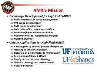
Probe card preparation. Y. Kwon (Yonsei Univ.) for EQENG, Notice, & Yonsei . Contents. PIN layout & pad definition from CERN Probe pin layout plan Schematics for probe card circuit Transparent chuck under consideration. PAD layout. Total 103 pads to make contact. PAD size.

E N D
Probecard preparation Y. Kwon (Yonsei Univ.) for EQENG, Notice, & Yonsei
Contents • PIN layout & pad definition from CERN • Probe pin layout plan • Schematics for probe card circuit • Transparent chuck under consideration
PAD layout Total 103 pads to make contact
PAD size We want dual pin contact for each pad.
Needlelayout Invisible Chip
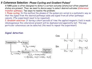
Specification 0. Dual pins for each pad Pin A for external connection (power/ground/IO), Pin B to check pin contact with the pad 1. 103 x 2 = 206 pins. 2. 14 + 3 relays as switches when we decouple pin A and pin B 3. 8 LEDs to check probe card position by eye. 4. Contact status check at every 10 ms. 5. Contact status report by ethernet.
Algorithm to check contact Disconnect power/input using relay. Send 1.8(V) logicpulse to each digital input pad via pin A and read pin B. If no pair read back, raise chuck via . If any pair reads back, 3. Start careful adjustment ’. 4. Send 1.8(V) sequential logic pulse to other digital input pad via pin A and read pin B. Raise ’ up until all input pad pairs read back. Send 1.8(V) sequential logic pulse to digital input pads via pin A and read pin B. (We will skip step 6 if we worry damage by electrical shock).
7. Raise ’ up until all input pad pairs read back. 8. FPGA pull down for power pin B, FPGA pull up for ground pin B. 9. Disconnect FPGA output for pin A. 10. Connect power. 11. Check FPGA pin status 12. Raise ’ up until all pin B status is OK. 13. Disconnect pin B for analog input. Use LED to display current status properly. FPGA flexibility enables variation of algorithm.
Pin A Pin B Input
Pin A Pin B Output
Pin B’s Power
Pin B’s Ground
Chucks in preparation Optimum number of vacuum holes to be decided.
Summary • Probe pin layout investigated. • Probe card schematics ready. • Transparent chuck in preparation.