Download
1 / 12
120 likes | 267 Views
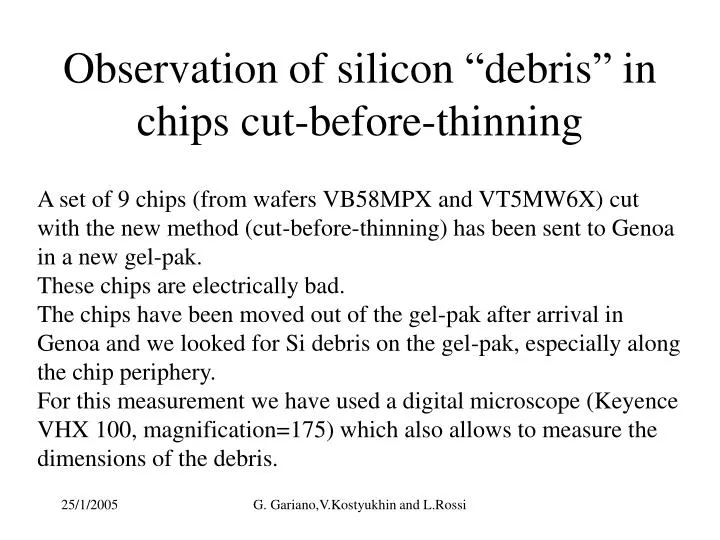
Observation of silicon “debris” in chips cut-before-thinning. A set of 9 chips (from wafers VB58MPX and VT5MW6X) cut with the new method (cut-before-thinning) has been sent to Genoa in a new gel-pak. These chips are electrically bad.

E N D
Observation of silicon “debris” in chips cut-before-thinning A set of 9 chips (from wafers VB58MPX and VT5MW6X) cut with the new method (cut-before-thinning) has been sent to Genoa in a new gel-pak. These chips are electrically bad. The chips have been moved out of the gel-pak after arrival in Genoa and we looked for Si debris on the gel-pak, especially along the chip periphery. For this measurement we have used a digital microscope (Keyence VHX 100, magnification=175) which also allows to measure the dimensions of the debris. G. Gariano,V.Kostyukhin and L.Rossi
Debris are along a (horizontal) line. Typical dimension is very small (few mm), some are 25-30 mm in radius. The center of the two large debris is 989 mm apart. G. Gariano,V.Kostyukhin and L.Rossi
Here another dangerous debris (same picture as in previous page), 20 mm in diameter. G. Gariano,V.Kostyukhin and L.Rossi
53x24mm 62x22mm There are debris for ~1mm, then few mm without appreciable number of debris. G. Gariano,V.Kostyukhin and L.Rossi
40x19mm Another example, still following an horizontal line. We could not see as clearly lines of debris along the vertical edges of the chips, only some debris are visible here and there. G. Gariano,V.Kostyukhin and L.Rossi
In the next two pages, the situation with the old cutting procedure is shown for comparison. These pictures, taken with a standard high magnification microscope, have been already circulated in July04 G. Gariano,V.Kostyukhin and L.Rossi
X 1000 G. Gariano,V.Kostyukhin and L.Rossi
Pictures taken at x1000 (see bump for comparison) 2 pictures showing fragments along the edge of a chip (now taken out). X 200 X 100 G. Gariano,V.Kostyukhin and L.Rossi
We find a couple of >10 mm dia (i.e. dangerous) debris per mm along the horizontal line close to the EoC logic. The distribution is not uniform (i.e. there are “regions of debris”). Some debris are present around the other sides, but there is no evidence of “lines of debris” as those shown in this report. The number of dangerous debris per mm is one order of magnitude less. This may be related to the way the chip is taken in/out from the gel-pak. The comparison with the previous cutting procedure indicate smaller debris and possibly less per mm. The improvement does not appear to be very significant because the smaller debris are in several cases still large enough to create VDDA problems. The edge of an “old” and a “new” chip has been compared then. G. Gariano,V.Kostyukhin and L.Rossi
New cutting Old cutting 40x Bump side Bump side G. Gariano,V.Kostyukhin and L.Rossi
Again there is no evidence of difference between the edges. The new cut procedure seems, in this case, slightly worse than the old one contraddicting other observations. It would be good to observe the same chip edge before leaving LBNL and after arrival in Genoa. A larger detail (next page) indicate that silicon debris of several tens of microns can fly off the edge on the side opposite to the bumps (so no surprise if we find them on the gel-pak). G. Gariano,V.Kostyukhin and L.Rossi
A 1000x picture of the edge of a new-cut chip (0208A of wafer VT5MW6X), The size of the chipping can be compared with a bump (below). G. Gariano,V.Kostyukhin and L.Rossi