Download
1 / 15
150 likes | 346 Views
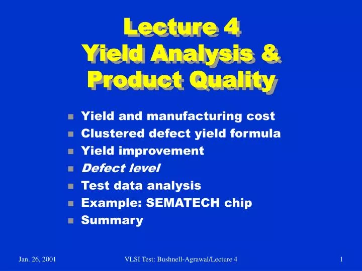
Lecture 4 Yield Analysis & Product Quality. Yield and manufacturing cost Clustered defect yield formula Yield improvement Defect level Test data analysis Example: SEMATECH chip Summary. VLSI Chip Yield.

E N D
Lecture 4Yield Analysis & Product Quality • Yield and manufacturing cost • Clustered defect yield formula • Yield improvement • Defect level • Test data analysis • Example: SEMATECH chip • Summary VLSI Test: Bushnell-Agrawal/Lecture 4
VLSI Chip Yield • A manufacturing defect is a finite chip area with electrically malfunctioning circuitry caused by errors in the fabrication process. • A chip with no manufacturing defect is called a good chip. • Fraction (or percentage) of good chips produced in a manufacturing process is called the yield. Yield is denoted by symbol Y. • Cost of a chip: Cost of fabricating and testing a wafer -------------------------------------------------------------------- Yield x Number of chip sites on the wafer VLSI Test: Bushnell-Agrawal/Lecture 4
Clustered VLSI Defects Good chips Faulty chips Defects Wafer Clustered defects (VLSI) Wafer yield = 17/22 = 0.77 Unclustered defects Wafer yield = 12/22 = 0.55 VLSI Test: Bushnell-Agrawal/Lecture 4
Yield Parameters • Defect density (d) = Average number of defects per unit of chip area • Chip area (A) • Clustering parameter (a) • Negative binomial distribution of defects, p(x ) = Prob (number of defects on a chip = x ) G(a+x ) (Ad /a) x = ------------- . ---------------------- x ! G (a) (1+Ad /a) a+x where G is the gamma function a =0, p (x ) is a delta function (max. clustering) a = , p (x ) is Poisson distr. (no clustering) VLSI Test: Bushnell-Agrawal/Lecture 4
Yield Equation Y = Prob ( zero defect on a chip ) = p (0) Y = ( 1 + Ad / a ) - a Example: Ad = 1.0, a = 0.5, Y = 0.58 , Y = e - Ad Unclustered defects: a = Example: Ad = 1.0, a = , Y = 0.37 too pessimistic ! VLSI Test: Bushnell-Agrawal/Lecture 4
Defect Level or Reject Ratio • Defect level (DL) is the ratio of faulty chips among the chips that pass tests. • DL is measured as parts per million (ppm). • DL is a measure of the effectiveness of tests. • DL is a quantitative measure of the manufactured product quality. For commercial VLSI chips a DL greater than 500 ppm is considered unacceptable. VLSI Test: Bushnell-Agrawal/Lecture 4
Determination of DL • From field return data: Chips failing in the field are returned to the manufacturer. The number of returned chips normalized to one million chips shipped is the DL. • From test data: Fault coverage of tests and chip fallout rate are analyzed. A modified yield model is fitted to the fallout data to estimate the DL. VLSI Test: Bushnell-Agrawal/Lecture 4
Modified Yield Equation • Three parameters: • Fault density, f = average number of stuck-at faults per unit chip area • Fault clustering parameter, b • Stuck-at fault coverage, T • The modified yield equation: Y (T ) = (1 + TAf / b) - b Assuming that tests with 100% fault coverage (T =1.0) remove all faulty chips, Y = Y (1) = (1 + Af / b) - b VLSI Test: Bushnell-Agrawal/Lecture 4
Defect Level Y (T ) - Y (1) DL (T ) = -------------------- Y (T ) ( b + TAf ) b = 1 - -------------------- ( b + Af ) b Where T is the fault coverage of tests, Af is the average number of faults on the chip of area A, b is the fault clustering parameter. Afand b are determined by test data analysis. VLSI Test: Bushnell-Agrawal/Lecture 4
Example: SEMATECH Chip • Bus interface controller ASIC fabricated and tested at IBM, Burlington, Vermont • 116,000 equivalent (2-input NAND) gates • 304-pin package, 249 I/O • Clock: 40MHz, some parts 50MHz • 0.45m CMOS, 3.3V, 9.4mm x 8.8mm area • Full scan, 99.79% fault coverage • Advantest 3381 ATE, 18,466 chips tested at 2.5MHz test clock • Data obtained courtesy of Phil Nigh (IBM) VLSI Test: Bushnell-Agrawal/Lecture 4
Test Coverage from Fault Simulator Stuck-at fault coverage Vector number VLSI Test: Bushnell-Agrawal/Lecture 4
Measured Chip Fallout Measured chip fallout Vector number VLSI Test: Bushnell-Agrawal/Lecture 4
Model Fitting Chip fallout vs. fault coverage Y (1) = 0.7623 Chip fallout and computed 1-Y (T ) Measured chip fallout Y (T ) for Af = 2.1 and b = 0.083 Stuck-at fault coverage, T VLSI Test: Bushnell-Agrawal/Lecture 4
Computed DL 237,700 ppm (Y = 76.23%) Defect level in ppm Stuck-at fault coverage (%) VLSI Test: Bushnell-Agrawal/Lecture 4
Summary • VLSI yield depends on two process parameters, defect density (d ) and clustering parameter (a) • Yield drops as chip area increases; low yield means high cost • Fault coverage measures the test quality • Defect level (DL) or reject ratio is a measure of chip quality • DL can be determined by an analysis of test data • For high quality: DL < 500 ppm, fault coverage ~ 99% VLSI Test: Bushnell-Agrawal/Lecture 4