Download
1 / 21
210 likes | 213 Views
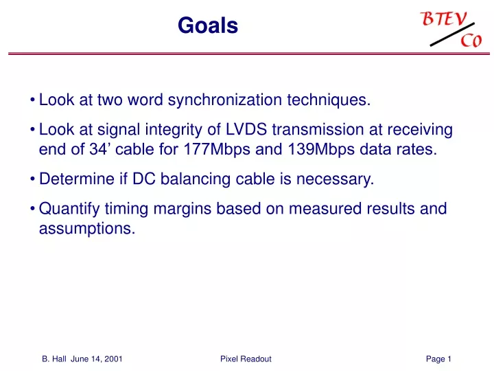
This study examines two word synchronization techniques for pixel readout, evaluates the signal integrity of LVDS transmission over a 34' cable at different data rates, and determines the need for DC balancing. The timing margins and skew caused by cable charging are quantified based on measured results and assumptions.

E N D
Goals • Look at two word synchronization techniques. • Look at signal integrity of LVDS transmission at receiving end of 34’ cable for 177Mbps and 139Mbps data rates. • Determine if DC balancing cable is necessary. • Quantify timing margins based on measured results and assumptions. Pixel Readout
Word Sync Method A Pixel Readout
Word Sync Method A Implementation of Word Sync Method A with DC balancing: With RCLK = 34.72Mhz, SCLK = 173.6Mhz (~174Mbps serial links) Pixel Readout
Word Sync Method A Implementation of Word Sync Method A with NO DC balancing: With RCLK = 34.72Mhz, SCLK = 138.88Mhz (~139Mbps serial links) Pixel Readout
Word Sync Method A • Simple to Implement • Receiver FPGA looks for leading ‘1’ to mark word boundaries. • FPGA can check for out of sync signs: illegal column address, more or less than 24 (or 30 in DC balance case) bit long words. • FPIX should transmit a sync word while data out of the core is idle. • Will need handshaking protocol allowing the receiver FPGA to request sync word transmission from FPIX. Pixel Readout
Word Sync Method B Pixel Readout
Word Sync Method B • A bit more complicated to implement: Pixel Readout
Word Sync Method B 6 serial lines would look like: Pixel Readout
Word Sync Method B One serial line configuration: Pixel Readout
Word Sync Method B • More logic required to implement. • Word sync every word…very fast recovery from transmission errors…should be very robust. • Must use 30 bits per word…177Mbps serial links. • Encoding also DC balances by allowing no more than 4 consecutive 0s or 1s (with NRZI). Pixel Readout
Signal Edge Skew Sources Pixel Readout
Data Edge Skew Sources Pixel Readout
Skew Due to Cable Charging • Use 34’ pleated foil flat cable (baseline for pixel system). • Inject LVDS signal at 177Mbps and 139Mbps. • Use pattern generator to transmit pattern with no DC balancing (up to 23 seq 0s or 1s) or a pattern with DC balancing (up to 4 seq 0s or 1s). • Look at received (LVDS to 3.3V CMOS) data and measure the signal edge movement due to cable charging. Pixel Readout
Cable Charging – 177Mbps No DC Balance Pixel Readout
Cable Charging – DC Balance: upto 4 seq 0s or 1s Pixel Readout
Cable Charging – 139Mbps No DC Balance Pixel Readout
Cable Charging – 139Mbps DC Balance: upto 4 seq 0s or 1s Pixel Readout
Cable Charging Conclusions • With 34’ cable @ 177Mbps or 139Mbps, DC balancing not critical. • @177Mbps and No DC balancing: skew = 2.53ns • @177Mbps and DC balancing: skew = 2.33ns • @139Mbps and No DC balancing: skew = 1.69ns • @139Mbps and DC balancing: skew = 1.69ns Pixel Readout
Other Contributions • FPIX pad to pad delay: 250ps (assumption) • Feedthrough board: 0ns (assumption) • Cable propagation delay variation (pair to pair): 1.3ns (previous study) • Cable charging: 1.69ns (@139Mbps, DC Balanced or not), 2.53ns (@177Mbps, No DC Balance), or 2.33ns (@177Mbps, DC Balanced up to 4 seq 0s or 1s) • Data combiner board: 0ns (assumption) • FPGA pin to pin delay: 250ps (assumption) • FPGA latch setup requirement: 800ps (Specification). Pixel Readout
Timing Margins (Clock Sampling Window) • With 177Mbps and No DC Balancing: 520ps • With 177Mbps and DC Balancing (4 seq): 720ps • With 139Mbps and No DC Balancing: 2.9ns • With 139Mbps and DC Balancing (4 seq): 2.9ns Also need to consider jitter of the clock itself. Pixel Readout
Conclusions/Discussion • 177Mbps has a good chance of not working. • 139Mbps has a good chance of working. • FPIX multiple serial line skew should be as tight as possible. • Word sync method A (leading 1 technique) will have to be used for 6 serial line configuration with 139Mbps. • Word sync method B (leading “00011” technique) can still be used for 1,2, or 3 serial line configurations (@139Mbps). Pixel Readout