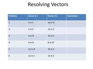
Download
1 / 17
170 likes | 211 Views
CdZnTe Energy Resolving Array Detectors Paul Seller Rutherford Appleton Lab. Acknowledgements:- Many thanks to Matt Wilson, Matt Veale and Lawrence Jones and others at RAL. Also thanks for the work illustrated here from the Universities of Surrey, Manchester and Durham.

E N D
CdZnTe Energy Resolving Array Detectors Paul Seller Rutherford Appleton Lab Acknowledgements:- Many thanks to Matt Wilson, Matt Veale and Lawrence Jones and others at RAL. Also thanks for the work illustrated here from the Universities of Surrey, Manchester and Durham. CZT Energy Resolving arrays
Material • CdTe is a black looking crystal • CZT has the Cd sites substituted for Zn. Mostly used as substrate for HgCdTe growth. (This substrate material is not detector grade.) • Typically detectors are TeCd1-xZnx ( x from 3% to 10%) • Piezo-electric crystal so inherently micro-phonic in parallel plate configuration. • Also Birefringent so can look at internal strains and fields with polarisers. • Hard and very brittle (handle with care). • Carcinogenic and accumulative. • Produced at 1100C by HP Bridgeman, Travelling Heater and Multi Tube Physical Vapour Transport (PVD). • Thin Layers by CSS or HWE 550C growth substrate but need to lattice match substrate. • CdTe Zinc–blend structure 3 inch Durham University CZT Energy Resolving CZT arrays
Properties • Band-gap CdTe= 1.5eV (Si =1.12eV) so room low leakage temperature semiconductor • This is equivalent to 820nm so transparent to IR light above this wavelength (can see defects with IR) • Zn added solely to increase Band-gap • Radiation conversion (w) factor = 4.4eV per electron hole pair (40keV photon gives 104 charge carriers) • Fano Factor =0.1 Eg = 1.505 + (0.631x) + (0.128x2) Photo luminescence map Band-gap and thus %Zn Energy Resolving CZT arrays
Radiation Absorption With thin layers watch the K-edge of Te and Cd at 22-27keV. Very high efficiency at 2mm thickness. Parallax With 500um of silicon stopping a 25keV beam a 250um voxel will have 2:1 parallax. A 100um layer of CZT will have 0.4:1 parallax. Energy Resolving CZT arrays
-bias X-ray h+ e- Pixels • Electron mobility 1000 cm2/Vs (Si=1400) • Hole mobility 50-80cm2/Vs (Si=480) • Carrier lifetime ~2us • mte ~2x10⁻³ cm2/V • mth ~2x10⁻⁴ cm2/V • (Holes take 2us to traverse 2mm) • Charge diffusion ~100um typical for 2mm thick • Bulk resistivity 3-9 x 10¹⁰ Ohm-cm (CdTe less) • Leakage current 1nA/mm2 (due to mid band states, reduced by Cl doping in CdTe, V or In in CZT) • Small pixel effect important to give single carrier output signal. (Improves speed and spectrum) Charge transport Shockley-Ramo theorem Energy Resolving CZT arrays
Contacts • CZT typically have Au or Pt contacts. Sputtered/evaporated pixels easy. • CdTe:Cl detectors now can have Indium rectifying anode contacts to reduce leakage and inter-pixel isolation. • Important to passivate sides to reduce leakage. • Need to remove surface damage (100-200um) and TeO layers before contacting. Etch with Br:Methanol. • Contacts increase resistance (less leakage than bulk) Energy Resolving CZT arrays
Manufacturers • Te precipitates and inclusions distributed in bulk, decorate twins and grain boundaries • These cause charge trapping and leakage. • At high fluxes the trapping (space charge) can distort the internal field and even stop operation (so-called polarisation). Need good hole transport to reduce this (mth >10-4 cm2/V) to get to >>10-6 counts/s/mm2 • Usually anneal the crystal in Cd vapour to reduce inclusions but it might still have trapping sites. • Watch operating temperature as low temperature increases trapping. • Can produce large CZT crystals with low trapping: • eV Products • Redlan • Bruker Baltic (only processing) • Orbotec • Durham University (CZT from Hexitec) • Acrorad (CdTe) • Kromek (CdTe) • Several Universities ???? Te precipitates Energy Resolving CZT arrays
Interconnect • Because CZT is very brittle and contacts are thin and fragile, difficult to use conventional ultrasonic wire bonding. • Most CZT devices do not like going above 150C or 120C for a long time. Probably due to redistribution of doping and diffusion of contacts. • So need a low temperature bonding process. • Other institutes use Indium bonding but in both cases have to watch diffusion. RAL ERD2004 system RAL low-temp Au-stud and Ag-epoxy method Energy Resolving CZT arrays
Energy Resolution Best resolutions on Bulk detectors being obtained are 0.8% FWHM dE/E with signal processing .(Zhong He below) Typically used for 100-700keV with either Coplanar-grid topology or double sided readout. To get this resolution one has to correct photopeaks for carrier trapping or use small pixel effect to reject hole signal. ERD2004 300um pixellated device. RAL. Am-241 energy spectrum taken at 278K and -400V. Np peaks visible between 10 and 30keV. The escape peaks of Te and Cd at 33 and 37keV respectively. Three-Dimensional Position Sensitive CdZnTe Detector Array for PNNL. Zhong He, et. al. University of Michigan wit h Gamma Medica ASIC. GE spectrometer with Rena-3 ASIC Energy Resolving CZT arrays
Spatial Resolution We believe this is due to charge steering in the array due to space charge in the device. Others suggest it is actually the charge trapping which causes the non-uniformity. Silicon on ERD2004, uniformity almost at level of statistics. CZT on same ERD2004 device highly non-uniform National Space Institute, Technical University of Denmark BNL. Bolotnikov et al. showing distorted internal fields in a thick detector. Energy Resolving CZT arrays
Examples of imaging systems • Si detectors readout holes, as high-resistivity Si wafers are usually n-type with p+ implanted pixels. • Holes are slow and get trapped in CZT so not good for pixellated readout. • ………..Need different pixellated readout electronics for CZT………… • Existing systems which synchrotron and HEP users are well aware of:- • Medipix 1-2-3 CERN et. al. • Pilatus PSI/Detris • XPAD CPPM Marseille • MPEC Bonn University • CMS tracker, Atlas tracker, old LEP experiments • Apart from CMS these are photon-counting with threshold not true energy resolving. Energy Resolving CZT arrays
Examples of imaging systems:- Ciemat , Acrorad (CdTe) Ciemat CSTD 300um pixel Compton camera system for medical imaging Bruker Baltic CZT Acrorad CdTe 4-side buttable100um pixels 50fps FPD. (Uses TSV technology on ASIC) Energy Resolving CZT arrays
Examples of imaging systems:- HEXITEC • UK funded program to: • make CZT material by MTPVT technique. • make this into detectors. • bond to an energy resolving imaging ASIC • ASIC is 80*80 pixels of 250um with 12 bit resolution spectroscopy up to 150keV (or 1.5MeV) • Maximum readout rate is 80Meg pixels/sec • Data acquisition system will sparcify data on fly and sends to PC by Camera-link • Durham, Surrey, Manchester, Birkbeck and STFC. 20*20 rolling shutter ASIC and camera-link based readout system (80*80) by summer Energy Resolving CZT arrays
Z. He et al, University of Michigan, IEEE NSS Conference Record, Hawaii 2007 Z. He et al, University of Michigan, IEEE NSS Conference Record, Hawaii 2007 Z. He et al, University of Michigan, IEEE NSS Conference Record, Hawaii 2007 Z. He et al, University of Michigan, IEEE NSS Conference Record, Hawaii 2007 Example:- PORGAMRAYS Compton Gama camera for security applications Portable Gamma Ray Spectrometer. Compton Imaging and Spectroscopy Partners: STFC DL and RAL, Universities of Liverpool and Manchester, John Caunt Scientific, Centronic, Corus. Funded by: EPSRC and TSB v Z. He et al, University of Michigan, IEEE NSS Conference Record, Hawaii 2007 CZT Energy Resolving Arrays
Cobra (Was Liverpool, Warwick, Sussex, Birmingham Universities +STFC) 1meter cube of CZT crystals to look for neutino-less doubleb decay as a test of the HEP Standard model. CZT is the source and the detector 1026 source atoms give one event per year so need 100kg Energy Resolving CZT arrays
Cobra • Need to put the CZT in a mine to shield background cosmic rays • Need to make CZT from isotopically enriched 116Cd • Need to track interactions in the detector volume to get 1-2% accuracy of 2.8MeV decay. Need <200um voxel resolution. • UK was proposing to use the PORGAMRAYS type technology. • PPRP review in the UK decided not to follow this. There is an international collaboration with other physicists and CZT scientists Energy Resolving CZT arrays