Download
1 / 18
180 likes | 187 Views
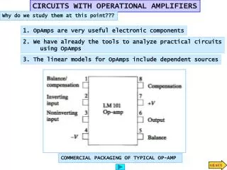
Operational Amplifiers Op Amps – a useful building block K. El-Ayat. 1. Op Amp: A DC coupled high Gain differential Amplifier Many useful applications. -ve. +ve. An Op Amp produces an output voltage that is much larger than the difference between its two inputs (very high gain).

E N D
Operational Amplifiers Op Amps – a useful building block K. El-Ayat 1
Op Amp: A DC coupled high Gain differential Amplifier Many useful applications -ve +ve An Op Amp produces an output voltage that is much larger than the difference between its two inputs (very high gain) Figure 2.2 The op amp shown connected to dc power supplies.
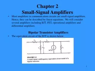
An Ideal Op Amp Differential input stage amplified • Infinite input impedance • Zero Output impedance • Infinite open-loop gain A • Infinite bandwidth Vout= A(v2-v1) • Op amps are DC (direct coupled) • Usually used with external components R, C, … Figure 2.3 Equivalent circuit of the ideal op amp.
Inverting Op Amp - Analysis Terminal 2 (+ve input) ground RF (or R2)connected to terminal 1 (-ve) Negative feedback Since open loop gain A very high Then v1-v2= vo/ A = 0 v1 = v2 = gnd VO = - (R2 / R1) * Vi i1 = i2 & Gain G = - R2 / R1 G (closed loop) gain Figure 2.6 Analysis of the inverting configuration. The circled numbers indicate the order of the analysis steps.
Op Amp – Class Analysis Example Find all I, v, gain v1 = i1 = i2 = vo = iL = io = Figure E2.6
An Op Amp Application; Weighted Summing Circuit in = ? i = ? vo = - [(Rf / R1) * v1 + (Rf / R2) * v2 +….+ (Rf / Rn) * vn] Figure 2.10 A weighted summer.
Two Op Amp comnibation Summing Circuit , with both signs Can calculate in 2 steps vo= v1(Ra/R1)(Rc/Rb) + v2(Ra/R2)(Rc/Rb) –v3(Rc/R3) –v4 (Rc/R4) Figure 2.11 A weighted summer capable of implementing summing coefficients of both signs.
Non inverting Op Amp Application Use +ve Op Amp input Figure 2.12 The noninverting configuration.
Non-inverting Op Amp: Analysis vo = vi + (vi/R1)*R2 vo = vi(1 + R2/R1) G = 1 + R2/R1 Figure 2.13 Analysis of the non-inverting circuit. The sequence of the steps in the analysis is indicated by the circled numbers.
Unity Gain Op Amp Voltage follower - unity gain; high current gain Buffer stage between processors - switches G = 1 + 0 /R1; R20 Figure 2.14 (a) The unity-gain buffer or voltage follower amplifier. (b) Its equivalent circuit model.
Op Amp problem – find vo I Assume x is voltage at both Amp inputs –ve, & +ve x = 3/5 (v1-v2) + v2 ; resistor divider I = x / 1 = (vo- x) / 9 vo = 10 x v o= 10 *[ 3/5 (v1-v2) + v2 ] = 6 v1 + 4 v2 ANS. Figure E2.9
Another Op Amp problem – Should be able to analyze vo = Figure E2.13
Can use as a difference Op Amp Figure 2.16 A difference amplifier.
Frequency response of Op Amp Gain = +10 Figure 2.23 Frequency response of an amplifier with a nominal gain of +10 V/V.
Open-loop gain of Op Amp Gain declines rapidly with freq Figure 2.22 Open-loop gain of a typical general-purpose internally compensated op amp.
Two-stage CMOS Op Amp - fyi Figure 9.1 The basic two-stage CMOS op-amp configuration.
Frequency Response of CMOS Op Amp fyi Figure 9.4 Typical frequency response of the two-stage op amp.
Inverting Op Amp Application to Impedances Figure 2.37 The inverting configuration with general impedances in the feedback and the feed-in paths.