Download
1 / 27
270 likes | 384 Views
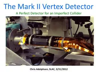
The Micro Vertex Detector for the Compressed Baryonic Matter Experiment. September, 7 – 9, 2011 St. Odile , France Joachim Stroth, Goethe-University Frankfurt / GSI f or the CBM-MVD collaboration. The CBM-MVD collaboration

E N D
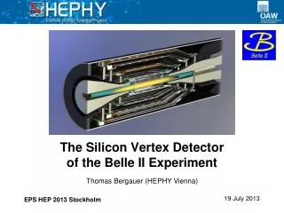
The Micro Vertex Detector for the Compressed Baryonic Matter Experiment September, 7 – 9, 2011 St. Odile, France Joachim Stroth, Goethe-University Frankfurt / GSI for the CBM-MVD collaboration
The CBM-MVD collaboration InstitutfürKernphysik, Goethe Universität Frankfurt am Main Samir Amar-Youcef, Norbert Bialas, Michael Deveaux, Dennis Doering, Melissa Domachowski, Christina Dritsa (now Univ. Giessen), Horst Düring, Ingo Fröhlich, Tetyana Galatyuk, Michal Koziel, Qiyan Li, Jan Michel, Boris Milanovic, Christian Müntz, Bertram Neumann, Paul Scharrer, Christoph Schrader, Selim Seddiki,Joachim Stroth, Tobias Tischler, Christian Trageser, Bernhard Wiedemann InstitutPluridisciplinaire Hubert Curien (IPHC), Strasbourg/France JérômeBaudot, GrégoryBertolone, Nathalie Chon-Sen, Gilles Claus, Claude Colledani, Andrei Dorokhov, WojchiechDulinski, Marie Gelin-Galivel, Mathieu Goffe, AbdelkaderHimmi, Christine Hu-Guo, KimmoJaaskelainen, Frédéric Morel, Fouad Rami, Mathieu Specht, Isabelle Valin, Marc Winter
Outline • RHIC physics at FAIR • The Compressed Baryonic Matter Experiment • Challenges for the Micro Vertex Detector • Design Principles • Mechanical Integration • Read-out • Sparsification and pre-processing
The FAIR accelerator Complex CBM/HADES APPA PANDA NuSTAR
Staged realization 2012: start of civil construction 2018: first beam • Modularized start version: • M0: SIS100 • M1: APPA • M1: CBM/HADES • M2: NuSTAR • M3: PANDA M0 M3 M1 M3 M2
Status of the SIS300 • Tunneldesignedtocontainbothsynchrotrons: SIS100+SIS300 • SIS100 fast ramping/cycling (11 AGeV Au) • SIS300 high energyandslowextraction(25A GeVAu)
Compressed Baryonic Matter at FAIR • Dedicated high-rate fixed target experiment • Compact tracking (silicon) in a 1 TM dipole field • Flexible arrangement of PID detectors • HADES for day-one experiments at SIS100 • Two experimentsat one single beam line
Transition Radiation Detectors Tracking Detector Electro- magnetic Calorimeter Muon detection System Ring Imaging Cherenkov Detector Silicon Tracking Stations Projectile Spectator Detector (Calorimeter) Vertex Detector Dipol magnet Resistive Plate Chambers (TOF)
First Level Event Selector V. Lindenstruth, J. de Cuveland et al. Frankfurt
Physics program of CBM Explore the nuclear phase diagram in the region of the first order phase transition Courtesyof T. Hatsuda
Rare and penetrating probes SPS Pb+Pb 30 A GeV Driving CBM experimental requirements in precision andrates
The CBM Physics Book The CBM Physics book is available now: Springer Series: Lecture Notes in Physics, Vol. 814 1st Edition., 2011, 960 p., Hardcover ISBN: 978-3-642-13292-6
Open Charm Measurements • Goal • comprehensive picture of charm production and propagation • Challenge • Rare probe • high precision displaced vertex reconstruction • Needs vertex detectors with • high resolution • minimal material budget • sufficient radiation tolerance • Calls for MAPS (MIMOSA-26 family) with high-resistivity epiand 180 nm technology. 300mm Silicon (equivalent)per layer!
Track Segment After all cuts applied (central 25 AGeV Au+Au) Identified e+e- (central 25 AGeV Au+Au) Identified e+/- Fakepair Track Fragment Low-mass Di-electrons • Goal • Excitaionfunctionofexcessyieldfrom 1 to 45 AGeV • Challenge • Background due to material budgetofthe STS • Sufficientpdiscrimination (missidentification <10-4) • Reductionofbackgroundbyreconstructingpairsfromg-conversionandp-Dalitz decay 8 per Au+Auevent 3 per Au+Auevent(central, 25 AGeV)
Experimental Challenges • General • High interactions rates (up to 100 kHz) with un-triggered (freely streaming) readout • Complex analysis on large data volume for First Level Event Selection (FLES) • MVD • Radiation tolerance (non-uniform irradiation): up to 1014neq(n.-ionizing) and 10 Mrad (ionizing) • Fast read-out (ultimately 10 ms) • Operation in vacuum, material budget determined by power dissipation • d-electrons
Occupancies and fluency Mean number of hits per mm2 and collision (station 1) Radiation tolerance: talk by Michael Deveaux
Intensity Fluctuations of Beam • Occupancy studies must take beam intensity fluctuation into account • Important also for on-chip buffer size • Peak to average values of extracted beam reach up to a factor 5 in 10 ms intervals at SIS100
Design Concept • Planar stations assembled from identical modules (not VELO-like) • Minimal material budget in the active area • Lateral heat extraction • Read-out components mostly on the periphery • 2 stations at 5 and 10 cm (+ one at 15 cm?) downstream of the target • First stations integrates2*5*4 = 40 sensors ~20 mm
Sensor Architecture • in-pixel pre-amp + CDS • column parallel read-out • binary charge encoding (?) • (switchable) zero-suppression • output buffers integrated at chip periphery • JTAG programmable • thinned to 50 μm
Heat evacuation (prototyping) Alternative: CVD diamond for 1. station Lateral heat evacuation feasible for 1W/cm2
Material Budget (prototyping) < 8 mm 10 mm active polyimide polyimide ~ 170 µm copper polyimide CVD ~150 µm: 0.11 % x/Xo polyimide copper polyimide polyimide
Prototype • Build a quarter of MVD-station 1 with ~0.3% X0 • Use MIMOSA-26 sensors • Develop scalable readout system based on HADES TRB system • Completion in 2012 Mechanical integration: talk by Tobias Tischler
DAQ concept Concept of the readout system of the prototype (2012) and the final MVD (2015) 2012 2012 340 Mbps LVDS MIMOSA-26 (MIMOSIS-1) Vacuum Window 340 Mbps LVDS 2012 2015 2015 340 Mbps optical Combiner Board (LVDS to optical conversion, 8/10 bit encoding in Ver. 2012) ~ 2 Gbps optical ~ 2 Gbps LVDS, 8/10 bit encoded Passive, radiation tolerant FEE-board 2015 - In Total: ~ 100 optical links: ~ 100 Gbps CBM DAQ Talks by Christoph Schrader and Jan Michel
Track Matching & Pattern recognition • Locally high occupancy due to • Event pile-up • d-electrons • MIMOSIS frame read-out (integration) time 30ms • STS time resolution 5 ns • Strategy: 4D track reconstruction in STS and extrapolation to MVD Time distribution of GEANT hits in detectors w.r.t. event t0
Cluster topology Open charm case. Distortion of reconstructed track due to eventually unidentified track fragment. Di-electron case: Find conversion/Dalitz partner to avoid combinatorial background hadron positron MVD2 electron MVD2 d-electron MVD1 MVD1 Talk by Christina Dritsa
Project status & plan • Demonstrator completed in 2009 • Two M20 seonsors on RVC/TPG compound • Prototype in 2012 • One quarter of MVD, M26 • Scalable read-out • Basis for (pre)TDR • First beam SIS100 earliest in 2018 • Time for second prototype with final sensor