Download
1 / 37
380 likes | 505 Views
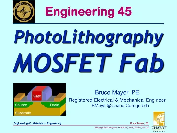
Engineering 45. PhotoLithography MOSFET Fab. Bruce Mayer, PE Registered Electrical & Mechanical Engineer BMayer@ChabotCollege.edu. silicon substrate. PhotoLithoGraphic Patterning - 1. Begin with a precise flat surface such as silicon wafer. field oxide. oxide. silicon substrate.

E N D
Engineering 45 PhotoLithographyMOSFET Fab Bruce Mayer, PE Registered Electrical & Mechanical EngineerBMayer@ChabotCollege.edu
silicon substrate PhotoLithoGraphic Patterning - 1 • Begin with a precise flat surface such as silicon wafer
field oxide oxide silicon substrate PhotoLithoGraphic Patterning - 2 • A THIN layer of a different material is deposited or grown on the substrate
PhotoLithoGraphic Patterning - 3 • A Thin layer of PHOTOsensitive, and acid/etch chemical RESISTING material (a.k.a. PhotoResist) is applied to the wafer photoresist oxide silicon substrate
Litho-4: Ultraviolet light Exposes photoresist through windows in a photomask Ultraviolet Light Chrome plated glass mask Shadow on photoresist Exposed area of photoresist photoresist oxide silicon substrate
Exposed area of photoresist Unexposed area of photoresist photoresist oxide silicon substrate PhotoLithoGraphic Patterning – 5 • Exposed photoresist becomes soluble and can be easily removed by a “developer” chemical.
photoresist photoresist oxide silicon substrate PhotoLithoGraphic Patterning – 6 • Unexposed photoresist remains on surface of oxide to serve as a temporary protective mask for areas of the oxide that are not to be etched/disolved
photoresist oxide oxide silicon substrate silicon substrate PhotoLithoGraphic Patterning – 7 • Areas of oxide protected by photoresist remain on the silicon substrate while exposed oxide is removed by the etching process.
Oxide Layer oxide oxide silicon substrate silicon substrate PhotoLithoGraphic Patterning – 8 • The photoresist is removed using a “stripping process” -- revealing the patterned “window” on the thin oxide layer.
Intel squeezes 2 BILLION transistorsonto new Itanium chip – Feb08 • The new 65-nanometer Tukwila Itanium processor, which is expected to be released at the end of 2009, will run at up to 2 GHz, have dual-integrated memory controllers and use Intel's QuickPath interconnect instead of a front-side bus. The processor also will have 2 billion transistors on one chip • BUT...What is a TRANSISTOR? • What KIND of Transistors are used? • HOW are the Transistors MADE?
Acknowledgement • These Following Images Were Graciously Provided by • Michael W. Davidson National High Magnetic Field Laboratory 1800 E. Paul Dirac Dr. The Florida State University Tallahassee, Florida 32310 Tel: 850-644-0542 Fax: 850-644-8920 email: davidson@magnet.fsu.edu web: http://microscopy.fsu.edu
n-MOSFET Electronic Device • negative channel, Metal-Oxide-Silicon, Field-Effect Transfer-resistor(Transistor) d g Vg s Gate Vs Source Electrical Current Vd Drain Drain
1. Form Gate & Isolation Dielectric • Oxidize P-Type Silicon in Tube Furnace • 1000-1100 °C in O2 or Wafer-Vapor • Forms Insulating Layer of Silicon Dioxide (SiO2) • Yellow Layer Below
2. Apply Photo Resist • Spin on “Thick” Liquid Photo Resist (blue) and “Soft-Bake” to make resist plastic-like
3. Expose the Negative PhotoResist • First Mask Placed Over PhotoResist • UltraViolet Light Projected onto the Mask • Exposed PhotoResist Hardens (negative resist)
4. Develop Exposed PhotoResist • Unexposed (and soft) PhotoResist (PR) is Washed away by the “Developer” Solution • Leaves the exposed PR and SiO2 in tact
5. Etch SiO2 to form Gate Dielectric • Etch the Thin the SiO2 Using “Plasma Etching” • Leave only a Very Thin Insulating Layer
6. Remove Used PhotoResist • Hardened PhotoResist is removed by one of: • Liquid Solvent • Gaseous Ozone “Ashing”
7. Deposit Gate Electrode Film • Deposit a Layer of Polycrystalline Silicon (red) by Low Pressure Chemical Vapor Deposition (LPCVD)
8. Apply 2nd Layer of PhotoResist • Cover PolySi with PhotoResist in Preparation for the Next Mask Step
9. Expose PhotoResist Using Mask-2 • The 2nd Mask is placed Over the PR • PR exposed to UV Light
10. Develop Gate Electrode PR • Use the Developer to Wash Away UnWanted PR • Leave Behind a “T” shaped PR pattern
11. Pattern Gate PolySilicon • Use “Dry” Plasma Etching Techniques to Remove BOTH PolySi and SiO2 in areas Not Protected by PR
12. Remove PR to Complete Gate Electrode • Remove PR by Ozone Ashing • Leaves a Strip of PolySi which Rises Above the Exposed Silicon
13. Change Exposed Si from P-type to N-type • Ion-Implant Phosphorus or Arsenic to Convert the Exposed Silicon to N-Type
14. Deposit Electrical Contact Insulation • Deposit SiO2 by TEOS+O3 APCVD • The SiO2 may P or P+B doped
15. Apply Contact Via PR • Apply a 3rd Layer of PhotoResist that Will be used to Form the Vertical Shafts used for Electrical Contacts
16. Expose PR using 3rd Mask • Again Exposed Masked PR to UV Light • The Black Rectangles Will Define the Contact Holes
17. Develop Contact-Via PR • Develop the PR to Expose the SiO2 in the desired Contract areas
18. Expose Silicon Thru Etching • Etch the SiO2 Not Protected by the PR to Expose the underlying Silicon • PolySi at rear • N-Type Si at Front-Left & Front-Right
19. Remove Contact-Via PR • Remove the PR to Reveal Contact holes, or vias, in the insulating APCVD-SiO2
20. Deposit Aluminum Contact Wiring • Blanket Deposit Al-Cu Alloy by Sputtering • Al Contacts the Si and PolySi thru the holes in the APCVD-SiO2
21. Apply “Wiring” PhotoResist • Apply a 4th Layer of PhotoResist that Will be used to Form the Al-Cu “wires” that Carry Electrical Current and Potential (Voltage) to the Transistor
22. Metallization Exposure • Expose the PR using the Metallization Mask
23. Develop Metallization PR • Develop PR Exposing Regions of the Al-Cu Metal for Subsequent Removal
24. Etch UnProtected Al-Cu to Form “Wires” • The Final Etching Step Removes the Unwanted Metal; Leaving only Metal used for • Contacting thru the Vertical-Shaft Vias the Silicon Source/Drain and Poly-Si Gate • Forming Strips of Al-Cu that act as Wires
25. Remove Remaining Resist Xsistor Done • Remove the Remaining Metallization Resist, Completing the n-MOSFET Transistor • Millions of transistors can be formed Simultaneously