Download
1 / 9
90 likes | 193 Views
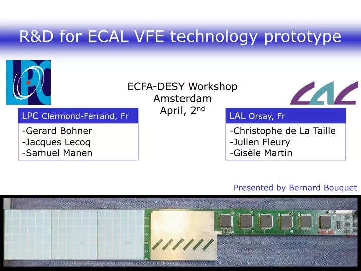
LPC Clermond-Ferrand, Fr. LAL Orsay, Fr. Gerard Bohner Jacques Lecoq Samuel Manen. Christophe de La Taille Julien Fleury Gisèle Martin. R&D for ECAL VFE technology prototype. ECFA-DESY Workshop Amsterdam April, 2 nd. Presented by Bernard Bouquet. General specifications.

E N D
LPC Clermond-Ferrand, Fr LAL Orsay, Fr • Gerard Bohner • Jacques Lecoq • Samuel Manen • Christophe de La Taille • Julien Fleury • Gisèle Martin R&D for ECAL VFE technology prototype ECFA-DESY Workshop Amsterdam April, 2nd Presented by Bernard Bouquet
General specifications Specifications General information Silicon-Tungsten calorimeter 40 layers 30 Millions channels Timing information 1 train every 200ms 3000 bunch crossing/train 1 bunch crossing every 154ns Signal information mechanic information Dynamic range : 15 bit Auto-triggered front end electronic • Electronic in the detector : • Thin design for room saving • Low consumption design Electrical specifications
General specifications Specifications Dynamic range 1 MIP 6.5fC Linearity below 1% up to 2500 MIP 14 or 15 bit dynamic range Number of channels/chip • Depending on the silicium wafer size Assuming 1 chip per wafer • 36 diodes per wafer at this point 36 channels per chip Noise specification Consumption specification 1 MIP 40,000 e- Noise expected to be below 2000 e- Detector is active only 1ms per 200ms Electronic enabled 2% of total inter-train time Electrical specifications
First ideas on block schema Schema Block Channel selection 6 Channel 12 BCID ADC Energy 3 BCID Ch.2 Gain 1 100 10 Ch.36 Further ideas on system design Ch.1
First ideas on block schema Schema Block ADC Shaper Bunch crossing counter 1 ADC/channel ? Consumption of ADC have to be < 1 mW Memorize after digitisation Use of digital memory instead of analogue New technology AMS 0.35µm BICMOS Using standard filter is not possible anymore due to technological problem high value resistance are not makable anymore LPC solution : A switchable integrator • LPC Will study digital memories +counter : • Static memory • Dynamic memory Further ideas on system design
Preamplifier Charge preamplifier Integration of the charge Due to a feedback capacitance Low noise, high speed design Input stage Middle stage Output stage Compensation capacitors Feedback capacitor Feedback resistor 1 50 OUT 1 50
Shaper OPA Preamp output Voltage to current converter R2 C2 C1 Preamp output R1 Standard CRRC structure Integration time (switch on) Standard bandpass filter optimized to minimize noise AMS 0.35µm BICMOS techno Does not allow us to choose this solution (R2 ~ 100k) Structure tested at LPC
ADC Behaviour • If VIN > Vref • Bit N out =1 and VIN N+1=(VIN-Vref)*2 • If VIN < Vref Bit N out =0 and VIN N+1=VIN*2 Structure tested at LPC : Chip should be sent to foundry in April 2003 PIPELINE ADC 10 bit ADC 10 stages VIN b7 b4 b3 b5 b8 b2 b1 b9 b0 b6 Amplifier Gain=2 To VIN stage N+1 Vref VIN Gnd Comparator Bit N out Vref Stage N of pipeline ADC block schema
Schedule LAL LPC • Input transistor • Preamplifier • 1 analogue channel • Foundry of pipeline ADC • VI conversion • Integrator shaper This year (depending on funding)