Download
1 / 39
460 likes | 1.35k Views
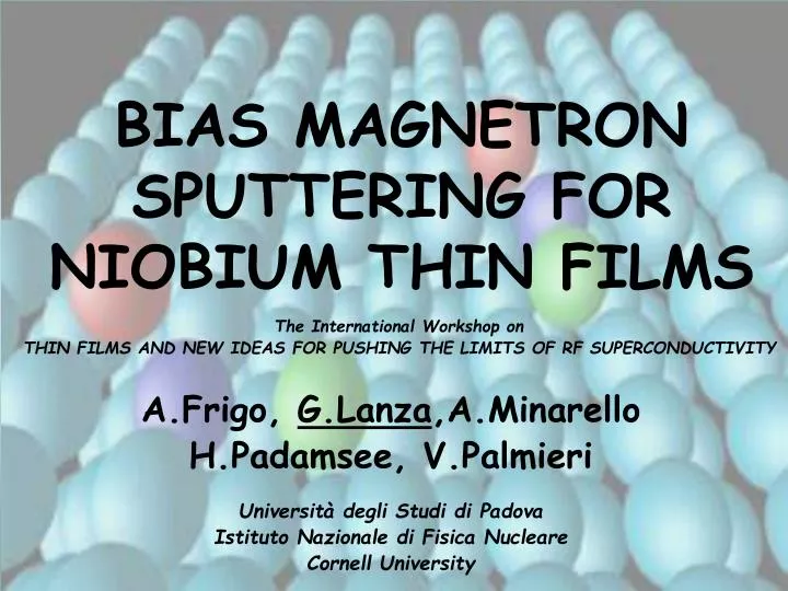
BIAS MAGNETRON SPUTTERING FOR NIOBIUM THIN FILMS. A.Frigo, G.Lanza ,A.Minarello H.Padamsee, V.Palmieri Università degli Studi di Padova Istituto Nazionale di Fisica Nucleare Cornell University. The International Workshop on

E N D
BIAS MAGNETRON SPUTTERING FOR NIOBIUM THIN FILMS A.Frigo, G.Lanza,A.Minarello H.Padamsee, V.Palmieri Università degli Studi di Padova Istituto Nazionale di Fisica Nucleare Cornell University The International Workshop on THIN FILMS AND NEW IDEAS FOR PUSHING THE LIMITS OF RF SUPERCONDUCTIVITY
Bias Magnetron Sputtering for Niobium thin films • Advantages and disadvanteges of the bias tecnique • Preliminary results of a mixed bias-magnetron sputtering configuration for coating Niobium on copper 1.5 GHz cavities • First applications of a large area cavity shaped cathode in the bias diode sputtering configuration.
Bias Sputtering The positive bias applyed to the grid between target and substrates promotes IONIC BOMBARDMENT OF THE GROWING FILM - Target + Biased Grid Substrate
Diode Bias Sputtering IONIC BOMBARDMENT OF THE GROWING FILM
Diode Bias Sputtering Impurities re-sputtering during the film growth
Diode Bias Sputtering Impurities are preferentially removed relative to the atoms of the main film. fraction of impurities trapped into the film i = impurities sticking coefficient Ni = atoms impurities arriving on the film β= function of the bias current due to impurities ions R= sputtering rate L.I.Maissel, P.M.Schaible; J.Appl.Phys. 36, 237 (1965)
Advantages • Densification of the crystal structure • Higher sputtering rate • Lattice rearrangement • Films quality improvement
Advantages • Increasing of the coating hardness • Similar defect annealing as does an elevated substrate temperature (E.Kay,G.Heim;J.Appl.Phys 49 (9) 4862 (1978)) • Electrons bombardment reduction • Adhesion improvement
Disadvantages • Noble gas atoms embedding • Lattice defects • Thickness reduction • Biased grid shadowing • Still hydrogen removal is low
Bias Sputtering 500Å 1000Å 5000Å Ta Resistivity (microhom-cm) High Resistivity Cathode Ta Resistivity (microhom-cm) Low Resistivity Cathode Substrate Bias (Volts) Substrate Bias (Volts) High bias voltage reduce differences between films sputtered from different cathodes and of different thickness. (Tantalum films studies-L.I.Maissel,P.M.Schaible,J.Appl.Phys. 36,237 (1965) )
The Niobium case Ta Resistivity (microhom-cm) Temperature coefficient of resistance (x10-3) Negative Bias Potential (Volts) Electrical resistivity and temperature coefficient of resistance of niobium films deposited on negatively biased substrates as a function of bias potential. ( J.Sosniak,J.Appl.Phys. 39,4157 (1968) )
The Niobium case Ic R Ib Film Deposition Rate Å/min Current (milliamperes) Negative Bias Potential (Volts) Deposition rate increases with increasing negative bias. (J.Sosniak,J.Appl.Phys. 39,4157 (1968) )
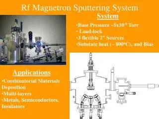
Standard CERN coating configurations Magnet Cylindrical Magnetron Cavity Niobium cathode
Standard CERN coating configurations Cooling air Ceramic insulator Niobium cathode - 450 V Stainless steel vacuum chamber with cavity shaped sample holders Moving magnet Niobium sputtered atoms Glow discharge Argon entrance To the vacuum pumps
Biased Grid +100 V INFN-LNL coating configuration Cathode - 250 V Magnet Grounded Cavity
Second Improvement Combination of the CERN coating configuration and the bias sputtering technique made from INFN-LNL - S N S Magnets S N N Target + Biased Grid Substrate
Water out Biased Magnetron Sputtering:the construction Improvement of the cooling system Water in
BIAS CERN type Biased Magnetron Sputtering: RRR results The grid still doesn’t affect much the equator part
BIAS CERN type Biased Magnetron Sputtering: thickness Sputtering rate obtained from thickness measurement
Biased Magnetron Sputtering: Tc results BIAS All samples with RRR>8 show a Tc higher than 9,3 K
Biased Magnetron Sputtering: lattice results BIAS Film show a lattice parameter lower than the Nb bulk They are grown with compressive stress
- Target + Biased Grid INFN-LNL coating configuration II The grid is behind the cathode Substrate
INFN-LNL coating configuration II The grid is behind the cathode • Advantages: • Anode-cathode distance reduction • Higher cathodic area • No shadowing due to the grid
A B Substrate Cathode BIAS INFN-LNL coating configuration II Plasma is conductive The bias grid can be placed behind the cathode
Bias Sputtering Bias CERN Low ratio cathode/substrate area Low sputtering rate (1 micron /day)
Cavity Shaped Cathode High ratio cathode/substrate area
Cavity Shaped Cathode Biased stainless steel tube Cathode -300 V Grounded Cavity Insulator
Cavity Shaped Cathode Vc = -300 V i = 5 A p = 6x10⁻²mbar
Summary • Mixed Bias Magnetron Sputtering • preliminary results (RRR, Tc, lattice) • studies with different bias and parameters • studies with shaped grid • test the cavity • Large Area Cavity Shaped Cathode • construction and first run • improvement of the structure stability • characterization of the films • test the cavity
to be continued… Thanks
INFN-LNL coating configuration Biased stainless steel tube Cathode -300 V Grounded Cavity Insulator
Cavity Shaped Cathode V=250 V i=8 A p=1x10⁻²mbar 10 cm 60 G