Download

1 / 27
270 likes | 841 Views
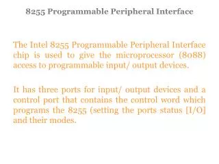
82C55 Programmable Peripheral Interface. Interfacing Part III. Review. More on Address decoding Interface with memory Introduction to Programmable Peripheral Interface 82C55. About 82C55.

E N D
82C55Programmable Peripheral Interface Interfacing Part III
Review • More on Address decoding • Interface with memory • Introduction to Programmable Peripheral Interface 82C55
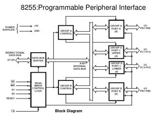
About 82C55 • The 82C55 is a popular interfacing component, that can interface any TTL-compatible I/O device to a microprocessor. • It is used to interface to the keyboard and a parallel printer port in PCs (usually as part of an integrated chipset). • Requires insertion of wait states if used with a microprocessor using higher that an 8 MHz clock. • PPI has 24 pins for I/O that are programmable in groups of 12 pins and has three distinct modes of operation.
Basic Mode Definitions and Bus Int • Mode 0 • Basic I/O • Mode 1 • Strobe I/O • Mode 2 • Bi-Dir Bus
Mode 0 (Basic Input/Output). • This functional configuration provides simple input and output operations for each of the three ports. • No “handshaking” is required, data is simply written to or read from a specified port.
82C55: Mode 0, Scan Display • Mode 0 operation causes the 82C55 to function as a buffered input device or as a latched output device. • In previous example, both ports A and B are programmed as (mode 0) simple latched output ports. • Port A provides the segment data inputs to display and port B provides a means of selecting one display position at a time. • Different values are displayed in each digit via fast time multiplexing.
MODE 1 (Strobed Input/Output) • This functional configuration provides a means for transferring I/O data to or from a specified port in conjunction with strobes or “handshaking” signals. • In mode 1, Port A and Port B use the lines on Port C to generate or accept these “handshaking” signals
Mode 1 Basic functional Definitions • Two Groups (Group A and Group B). • Each group contains one 8-bit data port and one 4-bit control/data port. • The 8-bit data port can be either input or output Both inputs and outputs are latched. • The 4-bit port is used for control and status of the 8-bit data port.
82C55: Mode 1 Strobed Input • ~STB : The strobe input loads data into the port latch on a 0-to-1 transition. • IBF : Input buffer full is an output indicating that the input latch contain information. • INTR : Interrupt request is an output that requests an interrupts. • INTE : The interrupt enable signal is neither an input nor an output; it is an internal bit programmed via the PC4 (port A) or PC2 (port B) bits. • PC7,PC6 : The port C pins 7 and 6 are general purpose I/O pings that are available for any purpose.
82C55: Mode 1 Strobed Input Signal definitions for Mode 1 Strobe Input
82C55: Mode 1 Input Exam. • Keyboard encoder debounces the key-switches, and provides a strobe whenever a key is depressed. • DAV is activated on a key press strobing the ASCII-coded key code into Port A.
82C55 : Mode 1 Output Exam. • ~OBF : Output buffer full is an output that goes low when data is latched in either port A or port B. Goes low on ~ACK. • ~ACK : The acknowledge signal causes the ~OBF pin return to 0. This is a response from an external device. • INTR : Interrupt request is an output that requests an interrupt. • INTE : The interrupt enable signal is neither an input nor an output; it is an internal bit programmed via the PC6(Port A) or PC2(port B) bits. • PC5,PC4 : The port C pins 5 and 4 are general-purpose I/O pins that are available for any purpose.
82C55: Mode 2 Bi-directional Operation • This functional configuration provides a means for communicating with a peripheral device or structure on a single 8-bit bus for both transmitting and receiving data (bidirectional bus I/O). • “Handshaking” signals are provided to maintain proper bus flow discipline in a similar manner to MODE 1. • Interrupt generation and enable/disable functions are also available.
MODE 2 Basic Functional Definitions: • Used in Group A only. • One 8-bit, bi-directional bus port (Port A) and a 5-bit control port (Port C). • Both inputs and outputs are latched. • The 5-bit control port (Port C) is used for control and status for the 8-bit, bi-directional bus port (Port A).
82C55: Mode 2 Bi-directional Operation • INTR : Interrupt request is an output that requests an interrupt. • ~OBF : Output Buffer Full is an output indicating that that output buffer contains data for the bi-directional bus. • ~ACK : Acknowledge is an input that enables tri-state buffers which are otherwise in their high-impedance state. • ~STB : The strobe input loads data into the port A latch.
82C55: Mode 2 Bi-directional Operation • IBF : Input buffer full is an output indicating that the input latch contains information for the external bi-directional bus. • INTE : Interrupt enable are internal bits that enable the INTR pin. BIT PC6(INTE1) and PC4(INTE2). • PC2,PC1,PC0 : These port C pins are general-purpose I/O pins that are available for any purpose.
82C55: Mode 2 Bi-directional Operation • Timing diagram is a combination of the Mode 1 Strobed Input and Mode 1 Strobed Output Timing diagrams.