Download
1 / 10
110 likes | 226 Views
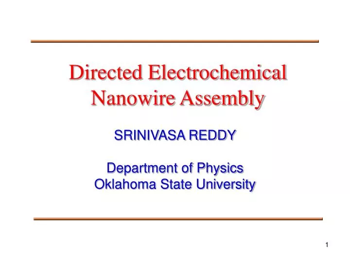
Directed Electrochemical Nanowire Assembly. SRINIVASA REDDY Department of Physics Oklahoma State University. Introduction. A critical issue in nanoscience is the conduction through very thin metallic wires.

E N D
Directed Electrochemical Nanowire Assembly SRINIVASA REDDY Department of Physics Oklahoma State University
Introduction • A critical issue in nanoscience is the conduction through very thin metallic wires. • As the wire diameter decreases the mean free path for conduction electrons decreases, leading to the inelastic collision of the electrons with the boundary surfaces of the metal. • Experimental verification of this issue is ambiguous and requires the fabrication of diameter-tunable, single-crystal, metallic nanowires with low contact resistance interfacing in the external circuitry.
Directed Electrochemical Nanowire Assembly (DENA) • Palladium wires from • palladium acetate solution.* • Developed DENA technique**: 20 mm • Single-step growth and interfacing of (near) single-crystalline metallic nanowires from simple salt solutions. *C. Cheng, R.K.G., Q. Gu, and D. T. Haynie, Nano Letters, 5, 175, 2005 **I. Talukdar, B. Ozturk, T.D. Mishima, B.N. Flanders, Appl. Phys. Lett., 88, 221907(2006) **B. Ozturk, D.R. Grischkowsky, T.D. Mishima and B.N. Flanders, Nanotechnology, 18, 175707 (2007)
Structural variation of indium wires 20 mm 20 mm 20 mm • Control of the growth voltage and solution concentration gives rise to • structural variation: (b) amorphous, (c) dendritic, (d) needle. I. Talukdar, B. Ozturk, T.D. Mishima, B.N. Flanders, Appl. Phys. Lett., 88, 221907.(2006)
Frequency dependent diameter 1.0 MHz 3.5 MHz 0.5 MHz 1 mm 1 mm 1 mm • SEM micrographs of indium wires grown with increasing growth frequency. I. Talukdar, B. Ozturk, B. N. Flanders, In preparation.(2007)
Frequency dependent diameter • As the growth frequency increases, the wire diameter decreases.
Frequency dependent velocity • Wire growth velocity increases with increasing frequency. • Velocity and diameter are anti-correlated: signature of dendritic • growth.* * G. P. Ivantsov, Dokl. Akad. Nauk.SSSR58, 567 (1947) J. S. Langer and H. Muller-Krumbhaar, Acta. Metall.26, 1961 (1978)
Conclusions • DENA technique allows the single-step growth and interfacing of • crystalline, metallic submicron wires from simply prepared solutions. • Wire diameter is tunable down to ~ 100 nm with the control of the • growth frequency. • These capabilities will facilitate future studies of diameter-dependent • transport measurements with the DENA technique. • We applied DENA technique to the growth of In, Ni, Au, Co, Cu, Ag, Zn and Pb wires.
Acknowledgements FUNDING NER-304413 EPS-132354 ECS-0601362 • Dr. Bret N. Flanders • Dr. Birol Ozturk • Prem Thapa