Download
1 / 32
320 likes | 443 Views
The World of Atoms. NCSU. Instructor: Dr. Gerd Duscher http:// www4.ncsu.edu/~gjdusche email: gerd_duscher@ncsu.edu Office: 2156 Burlington Nuclear Lab. Office Hours: Tuesday: 10-12pm Objective today: How do atoms arrange themselves ? Why is symmetry important ?

E N D
The World of Atoms NCSU Instructor: Dr. Gerd Duscher http://www4.ncsu.edu/~gjdusche email: gerd_duscher@ncsu.edu Office:2156 Burlington Nuclear Lab. Office Hours:Tuesday: 10-12pm Objective today: How do atoms arrange themselves ? Why is symmetry important ? Why do atoms break symmetry?
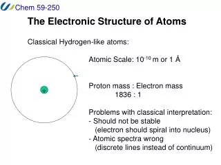
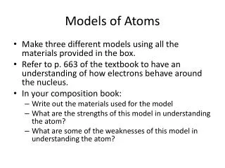
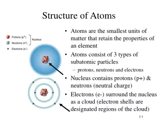
What is an Atoms? Bohr Model that is too simple
How do they bond? - Cl Cl + H H Ionic Bonding Covalent Bonding shared electrons H from carbon atom CH4 H H C shared electrons from hydrogen H Van Der Waals Bonding atoms arises from interaction between dipoles -ex: liquid HCl asymmetric electron clouds van der Waals - - + + bonding van der Waals bonding
What properties does that imply? • bond length, r • melting temperature, Tm Energy (r) F F r • bond energy, Eo r o r Energy (r) smaller T m unstretched length larger T m r o r E = Tm is larger if Eo is larger. o “bond energy”
Summary: Primary Bonds Ceramics large bond energy large Tm large E small a (Ionic & covalent bonding): Metals variable bond energy moderate Tm moderate E moderate a (Metallic bonding): Polymers directional Properties van der Waals bonding dominates small T small E large a (Covalent & Secondary): secondary bonding 18
Energy And Packing • Non dense, random packing energy typical neighbor bond length typical neighbor r bond energy • Dense, regular packing energy typical neighbor bond length r typical neighbor bond energy Dense, regular-packed structures tend to have lower energy.
Materials And Packing Crystallinematerials... • atoms pack in periodic, 3D arrays • typical of: -metals -many ceramics -some polymers crystalline SiO2 Noncrystalline materials... • atoms have no periodic packing • occurs for: -complex structures -rapid cooling "Amorphous"= Noncrystalline noncrystalline SiO2
Metallic Crystals • tend to be densely packed. • have several reasons for dense packing: -Typically, only one element is present, so all atomic radii are the same. -Metallic bonding is not directional. -Nearest neighbor distances tend to be small in order to lower bond energy. • have the simplest crystal structures. We will look at three such structures...
Simple Cubic Structure (sc) • rare due to poor packing (only Po has this structure) • close-packed directionsare cube edges. • Coordination # = 6 (# nearest neighbors)
Body Centered Cubic Structure (bcc) • Close packed directions are cube diagonals. --Note: All atoms are identical; the center atom is shaded differently only for ease of viewing. • Coordination # = 8
Face Centered Cubic Structure (fcc) • Close packed directions are face diagonals. --Note: All atoms are identical; the face-centered atoms are shaded differently only for ease of viewing. • Coordination # = 12
fcc Stacking Sequence • ABCABC... stacking sequence • 2D projection A B B C A B B B A sites C C B sites B B C sites • fcc unit cell 11
Hexagonal Close-Packed Structure (hcp) • ABAB... Stacking Sequence • 3D Projection • 2D Projection • Coordination # = 12 • APF = 0.74 12
Diamond Structure ZnS – type (GaAs) silicon, diamond
Structure Of Compounds: Nacl • Compounds: Often have similar close-packed structures. • Structure ofNaCl • Close-packed directions --along cube edges.
Perovskite Strucutre SrTiO3 Applications: non-linear resistors (PTC), SMD capacitors, piezoelectric sensors and actuators, ferroelectric memory.
Densities Of Material Classes Platinum Gold, W Tantalum Silver, Mo Cu,Ni Steels Tin, Zinc Zirconia Titanium Al oxide Diamond Si nitride Aluminum Glass - soda Glass fibers Concrete PTFE Silicon GFRE* Carbon fibers Magnesium G raphite CFRE * Silicone A ramid fibers PVC AFRE * PET PC H DPE, PS PP, LDPE Wood Graphite/ r r r Metals/ Composites/ metals ceramics polymers Ceramics/ Polymers Alloys fibers Semicond Why? Metals have... • close-packing (metallic bonding) • large atomic mass Ceramicshave... • less dense packing (covalent bonding) • often lighter elements Polymershave... • poor packing (often amorphous) • lighter elements (C,H,O) Compositeshave... • intermediate values 30 B ased on data in Table B1, Callister *GFRE, CFRE, & AFRE are Glass, 2 0 Carbon, & Aramid Fiber-Reinforced Epoxy composites (values based on 60% volume fraction of aligned fibers 10 in an epoxy matrix). ) 3 5 (g/cm 4 3 r 2 1 0.5 0.4 0.3 16
Crystals as Building Blocks • Some engineering applications require single crystals: --turbine blades --diamond single crystals for abrasives • Crystal properties reveal features of atomic structure. --Ex: Certain crystal planes in quartz fracture more easily than others.
POLYCRYSTALS • Most engineering materials arepolycrystals. 1 mm • Nb-Hf-W plate with an electron beam weld. • Each "grain" is a single crystal. • If crystals are randomly oriented, overall component properties are not directional. • Crystal sizes typ. range from 1 nm to 2 cm (i.e., from a few to millions of atomic layers).
Single vs Polycrystals E (diagonal) = 273 GPa E (edge) = 125 GPa • Single Crystals -properties vary with direction:anisotropic. -example: the modulus of elasticity (E) in bcc iron: • Polycrystals 200 mm -properties may/may not vary with direction. -if grains are randomly oriented: isotropic. (Epoly iron = 210 GPa) -if grains are textured, anisotropic.
TEMs at NCSU The NEW JEOL 2010F This is a TEM/STEM, which can do everything
TEMs at NCSU TEM Lab Course at the OLD TEM: Topcon
STEM at ORNL This STEM provides the smallest beam in the world. It uses the brightest source in the universe, 1000 times brighter than a supernova.
That is what happens when pulling wires. • before deformation • after tensile elongation slip steps Dislocation move, more dislocation get generated and entangle (interact) with themselfs, and other defects. Why?
Incremental Slip • Dislocations slip planes incrementally... • The dislocation line (the moving red dot)... ...separates slipped material on the left from unslipped material on the right. push Simulation of dislocation motion from left to right as a crystal is sheared. fixed
Bond Breaking And Remaking • Dislocation motion requires the successive bumping of a half plane of atoms (from left to right here). • Bonds across the slipping planes are broken and remade in succession. push Atomic view of edge dislocation motion from left to right as a crystal is sheared. fixed
Point Defects • Vacancies: -vacant atomic sites in a structure. • Self-Interstitials: -"extra" atoms positioned between atomic sites.
Point Defects In Alloys Two outcomes if impurity (B) added to host (A): • Solid solutionofBinA(i.e., random dist. of point defects) OR Substitutional alloy (e.g., Cu in Ni) Interstitial alloy (e.g.,CinFe) • Solid solution of B in A plus particles of a new phase (usually for a larger amount of B) Second phase particle --differentcomposition --often different structure. 8
Imaging of Single Bi Atoms in Si(110) A. Lupini, VG HB501UX with Nion Aberration Corrector, 100 kV
Types of Imperfections • Vacancy atoms • Interstitial atoms • Substitutional atoms •Anti-site defects Point defects (0 dimensinal) Line defects (1 dimensional) Area defects (2dimensional) • Dislocations • Grain Boundaries 2