Download
1 / 4
50 likes | 274 Views
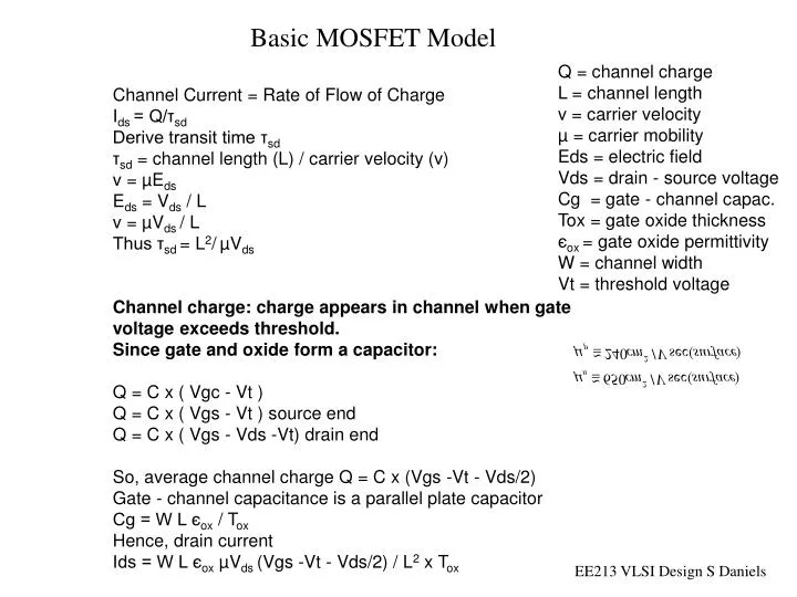
Basic MOSFET Model. Q = channel charge L = channel length v = carrier velocity µ = carrier mobility Eds = electric field Vds = drain - source voltage Cg = gate - channel capac. Tox = gate oxide thickness є ox = gate oxide permittivity W = channel width Vt = threshold voltage.

E N D
Basic MOSFET Model Q = channel charge L = channel length v = carrier velocity µ = carrier mobility Eds = electric field Vds = drain - source voltage Cg = gate - channel capac. Tox = gate oxide thickness єox = gate oxide permittivity W = channel width Vt = threshold voltage Channel Current = Rate of Flow of Charge Ids = Q/τsd Derive transit time τsd τsd = channel length (L) / carrier velocity (v) v = µEds Eds = Vds / L v = µVds / L Thus τsd = L2/µVds Channel charge: charge appears in channel when gate voltage exceeds threshold. Since gate and oxide form a capacitor: Q = C x ( Vgc - Vt ) Q = C x ( Vgs - Vt ) source end Q = C x ( Vgs - Vds -Vt) drain end So, average channel charge Q = C x (Vgs -Vt - Vds/2) Gate - channel capacitance is a parallel plate capacitor Cg = W L єox / Tox Hence, drain current Ids = W L єox µVds (Vgs -Vt - Vds/2) / L2 x Tox EE213 VLSI Design S Daniels
Basic MOSFET Model In the non - saturated region where Vds < Vgs - Vt K = єox µ/Tox = process transconductance parameter ß = KW/L = device transconductance parameter Saturation begins when Vds = Vgs - Vt In the saturated region where Vds = Vgs - Vt These expressions are based on a very simple model. Real transistors will behave slightly differently These expressions hold for both enhancement mode and depletion mode devices EE213 VLSI Design S Daniels
Threshold Voltage VSB = substrate bias voltage N = impurity concentration in the substrate Vt(0) = the threshold voltage for VSB = 0 Increasing VSB causes the channel to be depleted of charge carriers and thus the threshold voltage is raised Change in Vt depends on VSB and a constant which depends on substrate doping EE213 VLSI Design S Daniels
Transconductance Transconductance expresses the relationship between output current Ids and input voltage Vgs In saturation Vds = Vgs -Vt An indication of frequency response can be given by: This shows that switching speed is proportional to gate voltage above threshold and carrier mobility. Speed is inversely proportional to the square of the length of the channel Both gm and Vt are important FET characteristics which need to be tightly controlled EE213 VLSI Design S Daniels