Download
1 / 23
290 likes | 1.13k Views
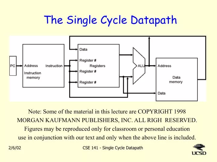
The Single Cycle Datapath. Note: Some of the material in this lecture are COPYRIGHT 1998 MORGAN KAUFMANN PUBLISHERS, INC. ALL RIGH RESERVED. Figures may be reproduced only for classroom or personal education use in conjunction with our text and only when the above line is included.

E N D
The Single Cycle Datapath Note: Some of the material in this lecture are COPYRIGHT 1998 MORGAN KAUFMANN PUBLISHERS, INC. ALL RIGH RESERVED. Figures may be reproduced only for classroom or personal education use in conjunction with our text and only when the above line is included. CSE 141 - Single Cycle Datapath
The Performance Big Picture • Execution Time = Insts * CPI * Cycle Time • Processor design (datapath and control) will determine: • Clock cycle time • Clock cycles per instruction • Starting today: • Single cycle processor: • Advantage: CPI = 1 • Disadvantage: long cycle time Execute an entire instruction CSE 141 - Single Cycle Datapath
PC Processor Design • We're ready to implement the MIPS “core” • load-store instructions: lw, sw • reg-reg instructions: add, sub, and, or, slt • control flow instructions: beq • First, we need to fetch an instruction into processor • program counter (PC) supplies instruction address • get the instruction from memory Address Write Enable Data In DataOut 32 32 Clk CSE 141 - Single Cycle Datapath
PC Processor Design • We're ready to implement the MIPS “core” • load-store instructions: lw, sw • reg-reg instructions: add, sub, and, or, slt • control flow instructions: beq • First, we need to fetch an instruction into processor • program counter (PC) supplies instruction address • get the instruction from memory 0 Address Write Enable instruction appears here Data In DataOut 32 32 Clk CSE 141 - Single Cycle Datapath
PC That was too easy • A problem – how will we do a load or store? • remember that memory has only 1 port • and we want to do everything in 1 cycle 0 Address Write Enable instruction appears here Data In DataOut 32 32 Clk CSE 141 - Single Cycle Datapath
Instruction & Data in same cycle? Solution: separate data and instruction memory There will be only one DRAM memory We want a stored program architecture How else can you compile and then run a program?? But we can have separate SRAM caches (We’ll study caches later) instruction appears here address Address Instruction cache Write Enable PC Data In DataOut Data Cache 32 32 Clk CSE 141 - Single Cycle Datapath
Instruction Fetch Unit Updating the PC for next instruction • Sequential Code: PC <- PC + 4 • Branch and Jump: PC <- “something else” • we’ll worry about these later CSE 141 - Single Cycle Datapath
31 26 21 16 11 6 0 op rs rt rd shamt funct 6 bits 5 bits 5 bits 5 bits 5 bits 6 bits 31 26 21 16 0 op rs rt immediate 6 bits 5 bits 5 bits 16 bits 31 26 21 16 0 op rs rt displacement 6 bits 5 bits 5 bits 16 bits The MIPS core subset • R-type • add rd, rs, rt • sub, and, or, slt • LOAD and STORE • lw rt, rs, imm • sw rt, rs, imm • BRANCH: • beq rs, rt, imm • Read registers rs and rt • Feed them to ALU • Update register file • Read register rs (and rt for store) • Feed rs and immed to ALU • Move data between mem and reg • Read registers rs and rt • Feed to ALU to compare • Add PC to disp; update PC CSE 141 - Single Cycle Datapath
Processor Design • Generic Implementation: • all instruction read some registers • all instructions use the ALU after reading registers • memory accessed & registers updated after ALU • Suggests basic design: CSE 141 - Single Cycle Datapath
31 26 21 16 11 6 0 op rs rt rd shamt funct 6 bits 5 bits 5 bits 5 bits 5 bits 6 bits Datapath for Reg-Reg Operations • R[rd] <- R[rs] op R[rt] Example: add rd, rs, rt • Ra, Rb, and Rw come from rs, rt, and rd fields • ALUoperation signal depends on op and funct CSE 141 - Single Cycle Datapath
31 26 21 16 0 op rs rt immediate 6 bits 5 bits 5 bits 16 bits Datapath for Load Operations R[rt] <- Mem[R[rs] + SignExt[imm16]] Example: lw rt, rs, imm16 CSE 141 - Single Cycle Datapath
31 26 21 16 0 op rs rt immediate 6 bits 5 bits 5 bits 16 bits Datapath for Store Operations Mem[R[rs] + SignExt[imm16]] <- R[rt] Example: sw rt, rs, imm16 CSE 141 - Single Cycle Datapath
Combining datapaths • How do we allow different datapaths for different instructions?? R-type Store CSE 141 - Single Cycle Datapath
Combining datapaths • How do we allow different datapaths for different instructions?? • Use a multiplexor! ALUscr CSE 141 - Single Cycle Datapath
31 26 21 16 0 op rs rt immediate 6 bits 5 bits 5 bits 16 bits Datapath for Branch Operations beq rs, rt, imm16 We need to compare Rs and Rt CSE 141 - Single Cycle Datapath
Computing the Next Address • PC is a 32-bit byte address into the instruction memory: • Sequential operation: PC<31:0> = PC<31:0> + 4 • Branch: PC<31:0> = PC<31:0> + 4 + SignExt[Imm16] * 4 • We don’t need the 2 least-significant bits because: • The 32-bit PC is a byte address • And all our instructions are 4 bytes (32 bits) long • The 2 LSB's of the 32-bit PC are always zeros CSE 141 - Single Cycle Datapath
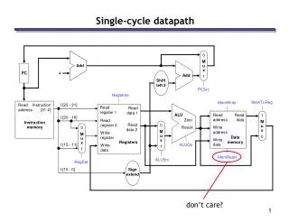
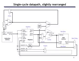
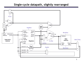
All together: the single cycle datapath CSE 141 - Single Cycle Datapath
The R-Format (e.g. add) Datapath Need ALUsrc=1, ALUop=“add”, MemWrite=0, MemToReg=0, RegDst = 0, RegWrite=1 and PCsrc=1. CSE 141 - Single Cycle Datapath
The Load Datapath What control signals do we need for load?? CSE 141 - Single Cycle Datapath
The Store Datapath CSE 141 - Single Cycle Datapath
The beq Datapath CSE 141 - Single Cycle Datapath
Key Points • CPU is just a collection of state and combinational logic • We just designed a very rich processor, at least in terms of functionality • Execution time = Insts * CPI * Cycle Time • where does the single-cycle machine fit in? CSE 141 - Single Cycle Datapath
Computer of the Day • The IBM 1620 (1959) • A 2nd generation computer: transistors & core storage (First generation ones used tubes and delay-based memory) • Example of creative architecture • ~ 2000 built. Relatively inexpensive ( < $1620/month rental) • A decimal computer – 6 bits per digit or character • 4 bits, flag (for +/- and end-of-word), ECC • Variable-length data – fields terminated by flag • Arithmetic by table lookup! • Codenamed CADET • “Can’t Add, Doesn’t Even Try” CSE 141 - Single Cycle Datapath