Download
1 / 14
160 likes | 197 Views
Electronic Physics. Dr. Ghusoon Mohsin Ali. Semiconductors Intrinsic In term of energy bands model, semiconductors can defined as that

E N D
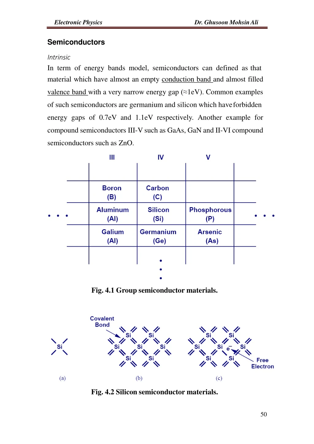
ElectronicPhysics Dr. Ghusoon MohsinAli Semiconductors Intrinsic In term of energy bands model, semiconductors can defined asthat material which have almost an empty conduction band and almost filled valence band with a very narrow energy gap (≈1eV). Common examples of such semiconductors are germanium and silicon which haveforbidden energy gaps of 0.7eV and 1.1eV respectively. Another example for compoundsemiconductorsIII-VsuchasGaAs,GaNandII-VIcompound semiconductors such asZnO. Fig. 4.1 Group semiconductormaterials. Fig. 4.2 Silicon semiconductormaterials.
ElectronicPhysics Dr. Ghusoon Mohsin Ali At 0 K there no electrons in conduction band and the Valence bandis completely filled, with increase temperature some of the electrons are liberated into conductionband. Fig. 4.3 Band diagram Si at 0 K and 300K Conductivity of semiconductor increase with temperature. Moreover for each electron(e) liberated into conduction banda positively charged hole(h) is created in the valence band. Semiconductor current consists of movement of electrons and holes in oppositedirections,supposethecovalentbondisbrokenatAandthe electron has moved through the crystal lattice leaving behind a hole in the covalent bond. An electron at B may jump into the vacant hole at A and later, an electron at C may jump into the hole at B and so on. In this way, by a succession of electron movements, a hole will appear at G and a negativechargewouldhavemovedfromGtoAItwould,howeverbemore convenient to regard positive charge to have moved from A to G and this conception gives rise to a hole as a positive charge carrier. It should be clearlyunderstoodthattheseholesareduetothemovementofelectronsin thevalencebandand.Thedriftvelocityofholesis,muchlessthanthedrift velocity ofelectrons. Anintrinsicsemiconductormaybedefinedasoneinwhichthenumberof conduction electrons is equal to the number ofholes.
ElectronicPhysics Dr. Ghusoon MohsinAli Fig. 4.4 Movement of holes in valanceband n p i i where ni is the number of electrons in the conductionband pi is the number of holes in the valenceband n2 np i i i The forbidden energy gap Egis E E E g c v Ec Eg Ev Fig. 4.4 Conduction band and valanceband Where Ec is the conduction band edgeand Ev is the valence band edge
ElectronicPhysics Dr. Ghusoon Mohsin Ali In a semiconductor, charge carriers are both electrons and holes (these arecalledthermally-generatedchargecarriers)thenthecurrentflowdueto the movement of electrons and holes in opposite direction. Even though the number of electrons equals the number of holes, hole mobility (μp) and electron mobility (μn) aredifferent. nepene() i n i p i n p J E ne()E i n p v 1E Dnn v E Dp p Example Calculate σ for pure Silicon if only one electron liberated from 1013 valence electrons, if density 2.33×10³kg/m3, atomic weight 28.086, μn=0.135 m2/Vs, μp=0.048 m2/Vs. Solution N Density NAvo 51028 /m3 Atomicweight No. of valence electrons= 4×5×1028=2×1029/m3 No. of conduction electrons=2×1029/ 1013=2×10¹⁶/m3 ni=pi=2×10¹⁶/ m3
ElectronicPhysics Dr. Ghusoon MohsinAli n e() 5.8104 S / m i n p Example A potential difference of 10 V is applied longitudinally to arectangular specimen of intrinsic Ge of length 2.5cm, width 0.4cm and thickness 0.15cm.Calculate (i) electron and hole drift velocities, (ii) σ of Ge if intrinsic carrier density is 2.5×10¹⁹/ m3, and (in) the total current, Given μn=0.38m2/Vs, μp=0.18m2/Vs . Solution (i) 10 v E 0.38 Dn n 152ms1 2.5*102 10 v E 018 Dp p 72ms1 2.5*102 (ii) ne() 2.24S /m i n p (iii) 10 IEA2.24 (0.40.15104)5.38mA 2 2.510 Physicalconstants Boltzmann's constant k=1.38×10⁻²³ J/K =8.62×10⁻⁵ eV/K Plank's constant h=6.625×10⁻³⁴ J.s =4.135×10⁻¹⁵eV.s kT=0.0259 eV
ElectronicPhysics Dr. Ghusoon MohsinAli The concentration of electrons in the conduction andis nN(E)fE,TdE Ec nNcexp((EcEF)/kT) 3 2m*kT2 N 2n h2 c where the parameter Nc is called the effective density of states function in the conduction band and its value is 2.8×1025/m3 for Silicon and 1.04×1025/m3 for Germanium and mn* is the effective mass of theelectron. Similarly the concentration of holes in the valence andis pNvexp((EFEv)/kT) 3 2m* kT2 N 2p h2 v The parameter Nv is called the effective density of states function in the valence band and its value is 1.04×1025/m3 for Silicon and 6×1024/m3 for Germanium, and mn* is the effective mass of thehole. For intrinsicsemiconductor ni=pi Ncexp((EcEF)/kT)Nvexp((EFEv)/kT)
ElectronicPhysics Dr. Ghusoon MohsinAli Nv exp(((Ec EF ) (E E))/kT) F v N c Nv exp((EcEFEFEv)/kT) N c N lnv(E E 2E ) /kT N c v F c N kTlnvE E 2E N c v F c E E N lnv kT cv 2 E 2 N F c The first term (Ec+Ev/2) is the energy exactly midway between Ec andEv or the midgapenergy E E cv 2 E midgap 3 2m*kT2 N 2n h2 c 3 m* 2m* kT2 E E 3 cv 2 N 2p E • kTlnp h2 m* v 4 F n m* 3 E E kTlnp m* 4 F midgap n
ElectronicPhysics Dr. Ghusoon Mohsin Ali wherem*istheeffectivemass,takeintoaccounttheparticlemassandalso takes into account the effect of the internal forces. If m *= m * thenthe n p intrinsic Fermi level is exactly in the center of the bandgap. If m *> m* the n p intrinsic Fermi level is slightly below the center. If mn*< mp* it is slightly above the center. Hence, the Fermi level of intrinsic semiconductor generally lies very close to the middle of bandgap. Example Calculate the position of the intrinsic Fermi level with respect to the center of the bandgap in silicon at T=300 K. The effective mass in silicon are mn*= 1.08m0 and mp*= 0.56m0. Solution The intrinsic Fermi level with respect to the center of the bandgapis m* 3 3 0.56 E E kTlnp0.0259ln m* 4 4 1.08 F midgap n E E 0.0128eV 12.8meV F midgap The intrinsic Fermi level in silicon is -12.8meV below the midgap energy. If we compare 12.8 meV to (1.12/2)=0.56eV =560meV. We may approximate that the intrinsic Fermi level to be in the center of the bandgap. The probability of the states not occupied by an electron is given as1- f(E,T). The function f(E,T) is symmetrical with the function 1-f(E,T) about the Fermi energy EF as shown in the figurebelow
ElectronicPhysics Dr. Ghusoon MohsinAli 1 1f(E,T) E E 1expF kT Example Determine the temperature at which there is a 1 percent that anenergy state 0.3 eV below the Fermi level isempty. Solution 1 1 f (E,T) EF E 1exp kT E EF 0.3 1 1 EF0.3EF0.3 100 1 99expexpkT kT 4.585120.3 kT Solving for kT, we find kT=0.0652 eV, so that the temperature isT=756. ==============================================
ElectronicPhysics Dr. Ghusoon MohsinAli E E E N(E) Ec f(E,T) 1-f(E,T) EF Ev N(E) E E N(E) N(E)f(E,T) Ec Electrons EF N(E)(1-f(E,T)) Holes N(E) Fig. 4.5 The density of states function N(E), the Fermi-Dirac distribution functionf(E),and areas representing electron and hole concentrations for the case when EF is near the midgap energy. We are assuming that the Fermi energy is within the forbidden energy band gap. For electrons in the conduction band. If we have, (E-Ec)>>kT. The Fermi probability function reduces to the Boltzmannapproximation. E E 1 f(E,T) expF EE F kT 1exp kT
ElectronicPhysics Dr. Ghusoon MohsinAli For energy states in the valence band, E<Ev. If (EF-Ev)>>kT. The Fermi probability function reduces to the Boltzmannapproximation. E E 1 1f (E,T) expF E E F kT 1exp kT Example Calculate the probability that a state in the conduction band is occupied by an electron and calculate the thermal equilibrium electron concentration in Si at T=300 K. If the Fermi energy is 0.25 eV below the conduction band. The value of Nc=2.8×1025/m3 atT=300K. Solution The probability that an energy state E=Ec is occupied by an electron is given by E E 1 f(E,T) expF EE F kT 1exp kT 0.25 5 f (E ,300) exp 6.4310 0.0259 c The electron concentration is givenby nNcexp((EcEF)/kT) n2.81025exp0.25/0.0259 n1.81021/m3 Example
ElectronicPhysics Dr. Ghusoon MohsinAli Calculate the thermal equilibrium hole concentration at T=400 K. Assume that the Fermi energy is 0.27 eV above the valence band energy. The value of Nv at T=300 K is1.04×1025/m3. Solution The parameter values at T=400K are foundas 4003/2 N 1.041025 1.61025/m3 v 300 400 kT 0.0259 0.03453eV 300 pNvexp((EFEv)/kT) p(1.61025)exp0.27/0.03453 p 6.431019 /m3 ============================================== The intrinsic carrier density is obtained from law mass ofaction ni2=np (E EF EF Ev)) 2 n N Nexp( c i c v kT ni NvNcexp((EcEv)/2kT) ni Nv Nc exp(Eg / 2kT)
ElectronicPhysics Dr. Ghusoon Mohsin Ali Example Calculate the intrinsic carrier concentration in gallium arsenide (GaAs) at T=300K and at T=450K. The values of Nc and Nv for GaAsare 4.7×10²³/m3 and 7×1024/m3, respectively. Both Nc and Nv vary as T3/2. If Eg of GaAs is 1.42 eV. Solution ni Nv Nc exp(Eg / 2kT) n4.7102371024exp(1.42/(20.0259)) i n 2.261012m3 i At T=450K 450 kT 0.0259 0.03885eV 300 4503 n4.7102371024exp(1.42/(2 0.03885)) i 300 n 3.851016m3 i
ElectronicPhysics Dr. Ghusoon Mohsin Ali Problems Q1: A bar of intrinsic silicon having a cross section area of 3×10⁻⁴ m2 has an ni=1.5×10¹⁶m-3. If µn=0.14 m2/V.s and µp=0.05 m2/V.s. Find the long of the bar if the current is 1.2mA and the applied voltage is 9V. (Ans:1.026mm) Q2: Calculate the thermal equilibrium electron and hole concentration in silicon at T=300K for the case when the Fermi energy level is 0.22 eV below the conduction band energy. Eg= 1.12 eV. The values of Nc and Nv are 2.8×1025/m3 and 1.04×1025/m3,respectively. (Ans: n=5.73×10²¹/m3,p=8.43×109/m3) Q3: Find the intrinsic carrier concentration in silicon at (a) T=200K, (b) T=400K. The values of Nc and Nv are 2.8×1025/m3 and 1.04×1025/m3, respectively. (Ans: (a) 7.68×10¹⁰/m3, (b) 2.38×10¹⁸/m3) Q4: Determine the position of the intrinsic Fermi level with respect to the center of the bandgap in GaAs at T=300K. mn*=0.067 m0, mp*=0.48 m0 (Ans:-38.2meV)