Download
1 / 6
70 likes | 153 Views
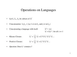
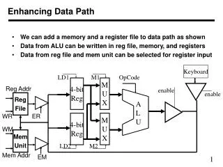
M- Reg. LDM. Input. OpCode. RA1. RA2. Reg File. EALU. EMR. EI. S H I F T. A L U. WM. Mem Unit. WR. WA. Mem Addr. EM. Operations on data path. An instruction specifies is a set of bit specifying an operation It includes control signals for

E N D
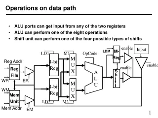
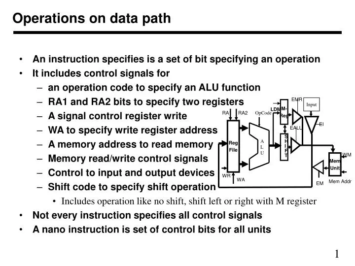
M- Reg LDM Input OpCode RA1 RA2 Reg File EALU EMR EI S H I F T A L U WM Mem Unit WR WA Mem Addr EM Operations on data path • An instruction specifies is a set of bit specifying an operation • It includes control signals for • an operation code to specify an ALU function • RA1 and RA2 bits to specify two registers • A signal control register write • WA to specify write register address • A memory address to read memory • Memory read/write control signals • Control to input and output devices • Shift code to specify shift operation • Includes operation like no shift, shift left or right with M register • Not every instruction specifies all control signals • A nano instruction is set of control bits for all units
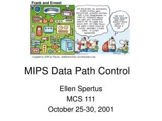
LD LD D3 D2 D1 D0 Q3 Q2 Q1 Q0 Clock LD LD LD D3 D2 D1 D0 D3 D2 D1 D0 D3 D2 D1 D0 Q3 Q2 Q1 Q0 Q3 Q2 Q1 Q0 Q3 Q2 Q1 Q0 D D D D Clk Clk Clk Q Q Q Q Q3 Q0 Q2 Q1 C C C C Clock Register file design • We will design an eight register file with 4-bit wide registers • A single 4-bit register and its abstraction are shown below • We have to use eight such registers to make an eight register file
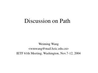
LD LD LD D3 D2 D1 D0 D3 D2 D1 D0 D3 D2 D1 D0 7 6 5 4 3 2 1 0 8-to-1 4-bit multiplex 7 6 5 4 3 2 1 0 8-to-1 4-bit multiplex Q3 Q2 Q1 Q0 Q3 Q2 Q1 Q0 Q3 Q2 Q1 Q0 RA1 RA2 Clk Clk Clk DATA1 DATA2 Reading circuit • To read any register, we need to multiplex the outputs • A 3-bit address, RA, specifies which register is to be read • The address is decoded to get the enable signal if using tri-state
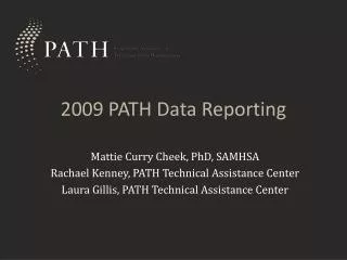
LD Data WA 3 to 8 D e c o d e r Reg LD Signal LD LD LD D3 D2 D1 D0 D3 D2 D1 D0 D3 D2 D1 D0 7 6 5 4 3 2 1 0 8-to-1 4-bit multiplex 7 6 5 4 3 2 1 0 8-to-1 4-bit multiplex Q3 Q2 Q1 Q0 Q3 Q2 Q1 Q0 Q3 Q2 Q1 Q0 RA1 RA2 Clk Clk Clk DATA1 DATA2 WR Adding write control to register file • To write any register, we need register address and a write signal • A 3-bit write address is decoded if write signal is present • One of the eight registers gets a LD signal from decoder
R R Q Q R G D P P Q S S S G P Q D P RS-latches and gated latch: a reminder • RS latch can act as a storage device • If R = 1 and S = 0, then Q goes to 0 and P goes to 1 • If R = 0 and S = 1, then P goes to 0 and Q goes to 1 • When R = 0 and S = 0, then P and Q remain where they are • Both R and S = 1 is a bad idea (for us) at the same time • These facts allow design of a gated latch with control signal G • G = 0 means no writing, G = 1 allows writing of input D
D D D D Q Q Q Q LD G G C C P P P P 2-to-1 Mux D IND C Edge-Triggered D-Flip-Flop: another reminder • Managing timing based on levels of signals is hard • We define a precise point in time when data gets stored • In an edge-Triggered flip-flop data is written on a clock edge • This is achieved by connecting two gated latches as below • When C is low, first latch gates data on D, second does nothing • When C goes high, the second latch latches Q of the first latch • A LD control can be added to load the new data or retain old data • D-latches also have a reset input to set Q output to zero Clock