Download
1 / 38
380 likes | 672 Views
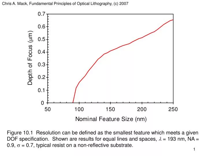
Figure 10.1 Resolution can be defined as the smallest feature which meets a given DOF specification. Shown are results for equal lines and spaces, l = 193 nm, NA = 0.9, s = 0.7, typical resist on a non-reflective substrate.

E N D
Chris A. Mack, Fundamental Principles of Optical Lithography, (c) 2007 Figure 10.1 Resolution can be defined as the smallest feature which meets a given DOF specification. Shown are results for equal lines and spaces, l = 193 nm, NA = 0.9, s = 0.7, typical resist on a non-reflective substrate.
Chris A. Mack, Fundamental Principles of Optical Lithography, (c) 2007 Figure 10.2 Comparison of the resolution for different feature types (l = 193 nm, NA = 0.9, s = 0.7). Here, L/S means equal lines and spaces.
Chris A. Mack, Fundamental Principles of Optical Lithography, (c) 2007 Figure 10.3 The definition of resolution can be used to study fundamental lithographic trends, such as the impact of numerical aperture (NA) on resolution (l = 193 nm, s = 0.7, equal lines and spaces).
Chris A. Mack, Fundamental Principles of Optical Lithography, (c) 2007 Figure 10.4 Resolution as a function of numerical aperture is more complicated than Rayleigh’s criterion would imply (l = 193 nm, s = 0.7, equal lines and spaces). Graphs show different resolution versus NA results for different minimum DOF specifications in nanometers.
Chris A. Mack, Fundamental Principles of Optical Lithography, (c) 2007 Figure 10.5 Examples of the three most common resolution enhancement technologies.
Chris A. Mack, Fundamental Principles of Optical Lithography, (c) 2007 Figure 10.6 The iso-dense print bias is fundamentally a result of the difference in the aerial images between isolated and dense lines. In this case, the isolated line is wider than the line in a dense array of equal lines and spaces (0.5 micron features, l = 365 nm, NA = 0.52, s = 0.5).
Chris A. Mack, Fundamental Principles of Optical Lithography, (c) 2007 (a) (b) Figure 10.7 Resist CD through pitch for different nominal feature sizes (used to fully characterize 1D proximity effects) can be very different as a function of the optical imaging parameters used: a) conventional illumination, s = 0.7, and b) quadrupole illumination, center s = 0.8 (l = 193 nm, NA = 0.85, binary mask, dose set to properly size the 100 nm line/space pattern).
Chris A. Mack, Fundamental Principles of Optical Lithography, (c) 2007 Figure 10.8 Proximity effects for different resist contrasts (400 nm nominal features, NA = 0.52, s = 0.5, i-line). The increasing pitch corresponds to increasing distance between 400 nm lines.
Chris A. Mack, Fundamental Principles of Optical Lithography, (c) 2007 Figure 10.9 Design curves of the mask linewidth bias (in wafer dimensions) required to make all of these features print at the nominal linewidth: 100 nm (thick line), 120 nm (thin line), and 140 nm (dashed line). Dose set to require no bias at 100 nm lines and spaces (l = 193 nm, NA = 0.93, s = 0.7, 6% ESPM).
Chris A. Mack, Fundamental Principles of Optical Lithography, (c) 2007 Figure 10.10 Discretized design curve (the stair-step approximation to the actual smooth curve) appropriate for use in a design rule table (5 nm correction grid used).
Chris A. Mack, Fundamental Principles of Optical Lithography, (c) 2007 (a) (b) Figure 10.11 A small section of a design a) before, and b) after correction of the middle feature with a simple 1D rule-based correction.
Chris A. Mack, Fundamental Principles of Optical Lithography, (c) 2007 (a) (b) Figure 10.12 A small section of a design a) before, and b) after the use of a simple 1.5 D rule-based correction.
Chris A. Mack, Fundamental Principles of Optical Lithography, (c) 2007 Figure 10.13 Example of model-based OPC: The original design (upper left) prints very poorly (upper right). After aggressive model-based OPC, the resulting design (lower left) prints very close to the desired shape (lower right). OPC and simulations done using PROLITH.
Chris A. Mack, Fundamental Principles of Optical Lithography, (c) 2007 (a) (b) Figure 10.14 Focus-exposure matrices (Bossung curves) for a) dense and b) isolated 130 nm features (isolated lines biased to give the proper linewidth at the best focus and exposure of the dense lines, l = 248 nm, NA = 0.85, quadrupole illumination optimized for a 260 nm pitch).
Chris A. Mack, Fundamental Principles of Optical Lithography, (c) 2007 (a) (b) Figure 10.15 Overlapping process windows generated from the focus-exposure matrices of dense and isolated lines for a) isolated lines with bias OPC (overlapping DOF = 300 nm) and b) isolated lines with scattering bars (overlapping DOF = 400 nm)
Chris A. Mack, Fundamental Principles of Optical Lithography, (c) 2007 Figure 10.16 Schematic diagram of SRAF placement showing the discontinuous effect of adding an SRAF as the pitch grows (main feature size is 100 nm).
Chris A. Mack, Fundamental Principles of Optical Lithography, (c) 2007 (a) (b) Figure 10.17 Off-axis illumination modifies the conventional imaging of a binary mask shown in (a) by tilting the illumination, causing a shift in the diffraction pattern as shown in (b). By positioning the shifted diffraction orders to be evenly spaced about the center of the lens, optimum depth of focus is obtained.
Chris A. Mack, Fundamental Principles of Optical Lithography, (c) 2007 Figure 10.18 The position within the lens of the diffracted orders from a pattern of lines and spaces is a function of the orientation of the lines and spaces on the mask.
Chris A. Mack, Fundamental Principles of Optical Lithography, (c) 2007 Figure 10.19 Various shapes for conventional and off-axis illumination.
Chris A. Mack, Fundamental Principles of Optical Lithography, (c) 2007 Figure 10.20 The impact of off-axis illumination on the log-slope defocus curve (NA = 0.85, l = 193 nm, binary chrome-on-glass mask, 120 nm lines and spaces). The dipole had a radius of 0.2 in sigma space.
Chris A. Mack, Fundamental Principles of Optical Lithography, (c) 2007 Figure 10.21 Quadrupole illumination optimized for a pitch of 200 nm showing how NILS varies with pitch both in-focus and with a moderate amount of defocus (NA = 0.85, l= 193 nm, 100 nm line, chrome-on-glass mask, quadrupole settings of 0.8/0.2).
Chris A. Mack, Fundamental Principles of Optical Lithography, (c) 2007 Figure 10.22 Quadrupole illumination optimized for a pitch of 200 nm showing how isolated lines do not show improved DOF (NA = 0.85, l= 193 nm, 100 nm line, chrome-on-glass mask, quadrupole settings of 0.8/0.2).
Chris A. Mack, Fundamental Principles of Optical Lithography, (c) 2007 Figure 10.23 Cross-section of a mask showing how the phase of the light transmitted through one part of the mask can be shifted relative to the phase of light transmitted through a nearby part of the mask.
Chris A. Mack, Fundamental Principles of Optical Lithography, (c) 2007 (a) (b) Figure 10.24 A mask pattern of equal lines and spaces of pitch p showing the idealized amplitude transmittance function and diffraction pattern for: a) binary chrome-on-glass mask; and b) alternating phase-shift mask.
Chris A. Mack, Fundamental Principles of Optical Lithography, (c) 2007 Figure 10.25 Cross-section of a mask of an isolated phase-shifted line.
Chris A. Mack, Fundamental Principles of Optical Lithography, (c) 2007 (a) (b) Figure 10.26 Behavior of an isolated phase-shifted line as a function of the chrome line width: a) coherent aerial images for w = 0 and 50 nm, and b) the aerial image width (at an intensity threshold of 0.25) as a function of the mask chrome width.
Chris A. Mack, Fundamental Principles of Optical Lithography, (c) 2007 (a) (b) Figure 10.27 Types of phase conflicts: (a) no phase shift across a critical pattern, and (b) the phase termination problem producing an unwanted phase edge.
Chris A. Mack, Fundamental Principles of Optical Lithography, (c) 2007 Figure 10.28 Simple example of a double-exposure alternating phase-shift mask approach to gate-level patterning.
Chris A. Mack, Fundamental Principles of Optical Lithography, (c) 2007 Figure 10.29 Example of a simple alternating phase-shift mask manufacturing approach.
Chris A. Mack, Fundamental Principles of Optical Lithography, (c) 2007 Figure 10.30 Intensity imbalance shown for an alternating phase-shift mask of equal lines and spaces.
Chris A. Mack, Fundamental Principles of Optical Lithography, (c) 2007 (a) (b) (c) Figure 10.31 Different approaches for fixing the phase error and intensity imbalance in alternating PSM: a) dual trench, b) undercut etch, and c) biased space.
Chris A. Mack, Fundamental Principles of Optical Lithography, (c) 2007 Figure 10.32 Cross-section of an attenuated PSM showing how the transmitted amplitude and phase of the light is modified by the attenuating material.
Chris A. Mack, Fundamental Principles of Optical Lithography, (c) 2007 Figure 10.33 An isolated space (100 nm, NA = 0.93, l = 193 nm, s = 0.5) imaged from a 6% attenuated PSM mask showing sidelobes.
Chris A. Mack, Fundamental Principles of Optical Lithography, (c) 2007 Figure 10.34 Impact of a twenty degree phase error on the aerial image of an isolated phase edge (l= 248 nm, NA = 0.75, s = 0.5).
Chris A. Mack, Fundamental Principles of Optical Lithography, (c) 2007 Figure 10.35 Aerial images for an alternating phase-shifting mask with a 10º phase error for +400 nm defocus (dots), no defocus (solid), and –400 nm of defocus (dashed). (100 nm lines and spaces with l = 248 nm, coherent illumination, 0.25 < k1 < 0.5).
Chris A. Mack, Fundamental Principles of Optical Lithography, (c) 2007 Figure 10.36 A small phase error in an EPSM mask changes the aerial image in the same way as a small shift in focus. Here, ±10º phase error moves the image closer and farther away from best focus (wavelength = 248 nm, NA = 0.8, 180 nm lines/space pattern, coherent illumination, 150 nm defocus). For this case, a 10º phase error shifts best focus by about 14 nm.
Chris A. Mack, Fundamental Principles of Optical Lithography, (c) 2007 Figure 10.37 Comparison of the ideal PSM from a chrome-on-glass (COG) mask and a 6% intensity transmittance embedded phase-shifting mask (EPSM).
Chris A. Mack, Fundamental Principles of Optical Lithography, (c) 2007 Figure 10.38 The aerial image of an isolated 180° phase edge (shown here using coherent illumination) will produce a narrow line in a positive resist.