Download
1 / 11
110 likes | 190 Views
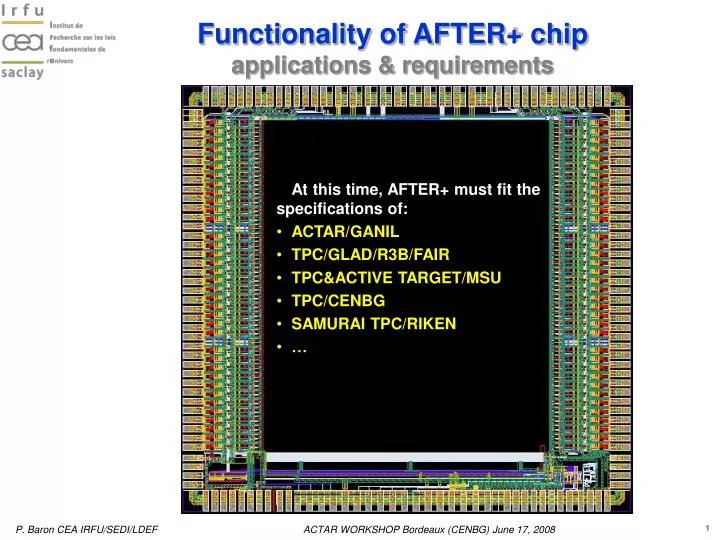
Functionality of AFTER+ chip applications & requirements. At this time, AFTER+ must fit the specifications of: ACTAR/GANIL TPC/GLAD/R3B/FAIR TPC&ACTIVE TARGET/MSU TPC/CENBG SAMURAI TPC/RIKEN …. AFTER+. Σ 72 discriminator outputs. hit channel registers. inhibit. 1 channel. DAC.

E N D
Functionality of AFTER+ chipapplications & requirements At this time, AFTER+ must fit the specifications of: • ACTAR/GANIL • TPC/GLAD/R3B/FAIR • TPC&ACTIVE TARGET/MSU • TPC/CENBG • SAMURAI TPC/RIKEN • …
AFTER+ Σ 72 discriminator outputs hit channel registers inhibit 1 channel DAC Discri Reset [hit channel registers] Charge range 76 to 1 FILTER SCA 12-Bit ADC CSA x72in 511 cells tpeak BUFFER Readout Mode Asic “Spy” Mode SCA MANAGER Power on Reset TEST SLOW CONTROL W / R CK In Test Serial Interface CKw & CKr CSA;CR;SCAin (N°1) Mode [+ indisc] AFTER+: Architecture [AD9229] Main features for AFTER+: • 72 Analog Channels; Slow Control & test [“spy” mode]. Main features for the channel • Input Current Polarity: positive or negative. • CSA + PZC + Filter (semi-Gaussian order 2). [Possibility to bypass the CSA]. • SCA: 511 analog memory cells. • Auto Triggering: discriminator + threshold (DAC) + inhibition. Main features for the readout • Analog OR of the 72 discriminator outputs [1 current output]. • Address of the hit channel (through slow control link). • 4 SCA readout modes. • Slow Control • Power on reset • Test mode: calibration or test[channel/channel] functional[72 channels in one step] • Spy mode on channel 1: CSAout, PZCout, FILTERout or DISCRIin.
Asic management (local or global) AFTER+ Trigger_out Trigger control: multiplicity & detection inhibit 1 channel DAC Reset Discri Reset: hit_channel register 76 to 1 SCA FILTER x72in 12-Bit ADC ADC control & Data CSA BUFFER SCA MANAGER TEST SLOW CONTROL Write Read SCA read: READ & CKread SCA write: Write & CKwrite Slow control: Din, Dout, CK, CS DAC Test: DAC SCA_in AFTER+: Mode of operation Stop Sampling:on external or local Trigger CSA_in Discri_in Channel i Discri_out Hit_channel Trigger_out Write_SCA Read_Address_hit channel Read_SCA Data_SCA_out Reset SCA write SCA read address read SCA write
76 lines In Bufferout 511 cells SCA write SCA read SCA Manager Clk write Clk read R W Vreturn:0,7V AFTER+: SCA Analog Memory: 72 channels + 4 dummy channels [for common mode or Fix pattern noise rejection purpose]. • Write: 1MHz to 100MHz • Read: 20MHz • Dynamic: 1.5V (full range) • Clock: LVDS • Mode (W & R): CMOS Write CLKwrite Read CLKread Write phase Read phase Write phase
c509 c510 c0 c1 c. ci-2 ci+2 ci-1 ci+1 ci channel ttrigger – tz=z0 ≤511 /Fsampling y DAC Discri tdriftz0 Cf tdriftz1 ttrigger particle x FILTER SCA t0= arrival time tdriftzmax z0 z1 CSA Ldrift Time pad Tz=zmax Tz=z1 Tz=z0 zmax 511 cells z tpeak PAD AFTER+: SCA Write Phase • Architecture : circular memory • Sampling condition : 511x(1/Fsampling) ≥ Tdriftmax • Peaking Time : Tpeak ≥ N x (1/Fsampling) • Fsampling: 1MHz to 100MHz. • Peaking Time: 50ns to 1µs (16 values).
Column n+1 Column n Address of the last Column read lumn n+510 Read_SCA CKR_SCA Column n+510 address Data_SCA_out Vreset Vreset Vlow Vlow C0 C1 C0 C1 C0 C1 C75 C75 C75 76xTrck 3xTrck 509x3xTrck 3xTrck 76xTrck + 509x76xTrck 9xTrck 9xTrck 61xTrck c509 c510 c0 ci-1 c1 ci+2 ci+1 ci-2 c. ci c509 c510 c0 ci-1 c1 ci+2 ci+1 ci-2 c. ci c509 c510 c0 ci-1 c1 ci+2 ci+1 ci-2 c. ci c509 c510 c0 ci-1 c1 ci+2 ci+1 ci-2 c. ci AFTER+: SCA Read Phase • Channel Readout mode : all channels; hit channels or specific channels Column n Channel 0 Readout Time: 511x [n channel + 3]xTrck + 79xTrck = 80.6 µs + 25.55 µsxnchannel [Trck = 50 ns] . n = 1 channel => Readout time = 106.15 µs. . n = 10 channels => Readout time = 336.1 µs. . n = 36 channels => Readout time = 1 ms. . n = 76 channels => Readout time = 2.022 ms. Channel 2 Channel n Channel 75
r/wb=1=> read Sc_din ADD<6:0> XXXXX X 1 Sc_ck Sc_en Sc_dout idle Address <71 :0> idle Y 8.5xTck:425ns 72xTck:3.6µs AFTER+: SCA Read Phase • Hit or specific channels: Slow control serial link & hit channel register (72 bits) Readout of the hit channel address Write_SCA Read_address_hit channel Write_address_read channel Read_SCA Clear r/wb=0=> write Sc_din Address Data <71 :0> 0 ADD<6:0> XXXXX X Write of the readout channel address Sc_ck Sc_en Sc_dout idle idle 7.5xTck:375ns 72xTck:3.6µs
AFTER+: SCA Read Phase • SCA readout mode: 511, 256 or 128 analog memory cells / channel • 511 analog memory cells / channel: Write phase Stop (trigger) Write phase: Tdrift ≤ 511 / Fsampling Read phase: SCAcells = 511 ci+1 510 ci 0 Readout phase • 256 analog memory cells / channel: Write phase Stop (trigger) Write phase: 2 x Tdrift ≤ 511 / Fsampling Read phase: SCAcells = 256 510 ci 0 Readout phase Internal Logical Operation • 128 analog memory cells / channel: Write phase Stop (trigger) Write phase: 4 x Tdrift ≤ 511 / Fsampling Read phase: SCAcells = 128 510 0 Readout phase
4-bit DAC 3-bit DAC OR_hit channel Iin Iin Iin Iin I=Iin I=Iin I=Iin I=Iin 72 xIin Hit channel 72 Hit channel i Hit channel 01 Hit channel 02 Iin Slow Control Register (2 bits) AFTER+: Threshold channel • Architecture: L.E.D + DAC (4 bits/channel + 3 bits/72 channels) SCA FILTER CSA PZC Analog out G2 511 cells Gain + 1 channel Discri Sign Memory Hit Channel - Polarity Inhibit • Trigger output: analog OR of the 72 hit channel registers. • Need specifications: • Current value • Rise & Fall time • Rout&Cout • Linearity (72*Iin ??)
Test: Charge injected channel by channel (selection 1/72 channel by Slow Control). [1 internal injection capacitor/charge range] Pulse Generator x72 Pulse Generator x72 seli selj selj selj seli seli X3 (1/Charge range) ASIC ASIC • Calibration: Charge injected channel by channel (selection 1/72 channel by Slow Control). x76 ASIC • Functionality of the global electronic system: Charge injected on all channels (or a part), at the same time. [in this mode, the FPN channels can be tested] Pulse Generator AFTER+: Architecture of the test system • 3 test modes: Test, Functionality & Calibration Ccali