Download
1 / 11
110 likes | 182 Views
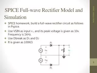
SPICE Simulation of Generalized Return Ratio (GRR ) vs. Loop Gain (LG). Trans-Impedance Amplifier (TIA). I C1 = 1 mA R C = 10 k Ω R F = 20 k Ω β = 200 V A = 1000 V R μ = 1 M Ω C π = 0.3 pF C μ = 100 fF C CS = 100 pF. GRR Simulation w/ Output Break Point. RR V. RR I.

E N D
SPICE Simulation ofGeneralized Return Ratio (GRR)vs. Loop Gain (LG)
Trans-Impedance Amplifier (TIA) IC1 = 1 mA RC = 10 kΩ RF = 20 kΩ β = 200 VA = 1000 V Rμ= 1 MΩ Cπ= 0.3 pF Cμ = 100 fF CCS= 100 pF
Loop-Gain Simulation Vtdriving at Input Vtdriving at Output Product of two voltage gains is the loop gain (why?)
*Generalized Return-Ratio Calculation *Comparison of RR to Loop-Gain Simulation *A simple model of BJT w/o capacitance .MODEL npn NPN +IS=1.0E-16 BF=200 VAF=1000 RB=0 *The basic TIA sub-circuit used in sim. .subckt TIA V1 V2 V3 V4 Q1 V2 V1 GND NPN M=1 Rmu V1 V2 1x Cpi V1 GND 0.3p Cmu V1 V2 100f Ccs V2 GND 100p RC VCC V2 10k RF V3 V4 20k *Bias up the circuit w/ ideal I and bypass C ICC GND VCC 1.005m CCC GND VCC 1 .ends TIA *Calculate the gen. RR *Break loop open at output, voltage drive XOV OV1 OV2 OV1 OV4 TIA LOV OV2 OV4 1e3 COV OV4 OV3 1 VOV OV3 GND AC=1 *Break loop open at output, current drive XOI OI1 OI2 OI1 OI4 TIA COI OI2 GND 1 LOI OI2 OI4 1e3 IOI GND OI4 AC=1 *Break loop open at input, voltage drive XIV IV1 IV2 IV3 IV2 TIA LIV IV1 IV3 1e3 CIV IV1 IV4 1 VIV IV4 GND AC=1 *Break loop open at input, current drive XII II1 II2 II3 II2 TIA LII II1 II3 1e3 CII II3 GND 1 III GND II1 AC=1 *Calculate the loop-gain w/ direct voltage drive XLI LI1 LI2 LI1 LI2 TIA CLI LI3 LI1 1 VLI LI3 GND AC=1 XLO LO1 LO2 LO1 LO2 TIA CLO LO3 LO2 1 VLO LO3 GND AC=1 .op .ac dec 10 1e3 1e12 *Derive RR from the gen. RR's @ output terminal .probe ac RRO=par('(v(OV2)*i(COI))/(v(OV2)+i(COI))') *Derive RR from the gen. RR's @ input terminal .probe ac RRI=par('(v(IV3)*i(CII))/(v(IV3)+i(CII))') *Derive loop-gain by multiplying two gains .probe ac LG=par('v(LI2)*v(LO1)') .option nomodnopagecaptab post acout=0 ingold=2 .temp 25 .end